
 My Inquiry
 My Account


Analog Devices Inc. ADP5350ACPZ-1-R7
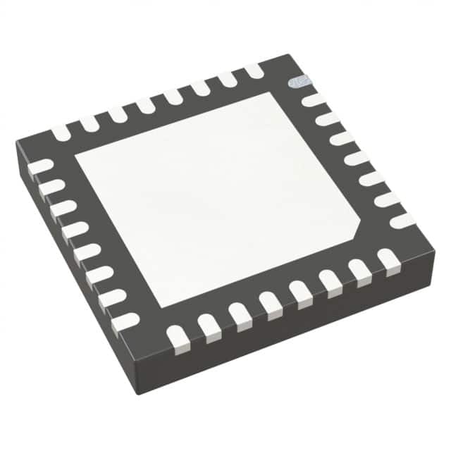
- Part No.:
- ADP5350ACPZ-1-R7
- Manufacturer:
- Analog Devices Inc.
- Category:
- Battery Management
- Package:
- 32-WFQFN Exposed Pad, CSP
- Datasheet:
-
 ADP5350ACPZ-1-R7.pdf
- Description:
- IC BAT PWR MGT LI-ION 1C 32LFCSP
- Quantity:
- Payment:

- Shipping:

Inventory:126
Please send an inquiry. Send us your inquiry, and we will respond immediately.
Product details
Overview
ADP5350ACPZ-1-R7 from Analog Devices is an advanced battery management PMIC integrating a 3 MHz buck charger, fuel gauge, 1.5 MHz boost LED driver with five independent current sinks (up to 20 mA each), and three 150 mA LDO regulators. It supports Li-Ion/Li-Poly battery charging with JEITA-compliant temperature regulation, voltage-based SOC estimation, and power-path control for system operation with dead batteries - used in wearable medical monitors and portable instrumentation.
For engineers reviewing the ADP5350ACPZ-1-R7 datasheet, ADP5350ACPZ-1-R7 pinout, ADP5350ACPZ-1-R7 application, or ADP5350ACPZ-1-R7 equivalent, this device delivers programmable charge termination (4.200 V ±0.3%), ultra-low quiescent current (1 µA typical for LDO1 at zero load), I²C-configurable LED blinking timers, adaptive headroom control for LED efficiency, and thermal shutdown at 140°C - critical for space-constrained, battery-sensitive designs.
Technical Context
The ADP5350ACPZ-1-R7 implements a dual-path power architecture: its 3 MHz buck regulator handles USB-input battery charging with internal FETs (RDSON_P = 280 mΩ, RDSON_N = 210 mΩ), while the 1.5 MHz boost converter supplies up to 16 V to drive LEDs in series or parallel configurations. The integrated 12-bit ADC enables voltage-based fuel gauge functionality with ±30 mV accuracy across −40°C to +85°C.
All regulation, timing, and protection functions-including JEITA thermistor thresholds (e.g., RCOOL_COLD = 151.2 kΩ), charge current (25–650 mA), and LED current levels (64 programmable steps)-are controlled via a 400 kHz I²C interface with dedicated interrupt (INT) and power-good (PGOOD) outputs. The device operates across −40°C to +125°C junction temperature and supports both LFCSP and WLCSP packages.
Key Specifications
| Parameter | Value and Actual Design Meaning |
|---|---|
| Buck Switching Frequency | 3 MHz - enables compact 1.5 µH inductor and low-profile 10 µF input capacitor (CFL1) for minimal PCB footprint. |
| Boost Switching Frequency | 1.5 MHz - supports high-efficiency white LED backlighting with adaptive headroom control reducing power loss in current sinks. |
| Charge Termination Voltage | 4.200 V ±0.3% - precise CV-mode cutoff ensures optimal Li-Ion cell longevity and safety compliance. |
| LDO1 Quiescent Current | 1 µA typical at zero load - extends battery runtime in always-on keep-alive rails (e.g., RTC or sensor bias). |
| LED Current Accuracy | ±10% at 20 mA - guarantees consistent brightness across all five channels without external calibration. |
| I²C Interface Speed | 400 kHz - allows real-time dynamic adjustment of charge parameters, LED dimming, and fault monitoring in embedded firmware. |
| Thermal Shutdown Threshold | 140°C rising - protects silicon integrity during sustained high-current LED or charging operation in sealed enclosures. |
Pinout & Package
The ADP5350ACPZ-1-R7 is housed in a 32-lead, 5 mm × 5 mm LFCSP package (CP-32-121), thermally optimized with θJA = 42°C/W and exposed paddle for PCB heat sinking. Pin functions are validated per Analog Devices Rev. B datasheet Figure 4 and Table 9.
| Pin/Terminal | Circuit Role | Design Meaning |
|---|---|---|
| INT | Active-low interrupt output | Signals charge completion, thermal warning, or LED fault - requires external pull-up; enables low-power polling-free system wake-up. |
| PGOOD | Open-drain power-good indicator | Asserts when regulated outputs (VOUT1/2/3 or VOUT4) meet 90% threshold - used for sequenced power enable in multi-rail systems. |
| THR | Thermistor input | Connects to NTC network (RNTC = 47 kΩ, BETA = 3800) for JEITA-compliant charge current derating across 0°C–45°C battery temperature range. |
| BSNS | Battery voltage sense | High-impedance input monitoring cell voltage for SOC calculation, termination, and short-circuit detection (VBAT_SHR = 2.4 V). |
| ISOB / ISOS | Isolation FET source/drain | Enables power-path control: ISOB powers system load, ISOS connects to USB input - permits operation with dead battery or hot-swap charging. |
| VIN123 | LDO1/2/3 input supply | Accepts 2.56–5.5 V; powers three independent 150 mA LDOs with programmable 1.0–4.2 V outputs and <120 µVrms noise. |
| VIN4 | Boost regulator input | 2.85–5.5 V input for 1.5 MHz boost stage; supports standalone operation or cascaded supply from LDOs or buck output. |
| FB4 | Boost feedback reference | 0.65 V ±1.5% reference - sets VOUT4 via external resistor divider; enables precise 5.6–18.5 V programmable OVP thresholds. |
Key Features
| Feature | Design Value |
|---|---|
| Integrated fuel gauge with voltage-based SOC | Eliminates need for coulomb counter IC or external sense resistor - reduces BOM count and PCB area in wearables and portable diagnostics. |
| Programmable LED current sinks (5×) | Each sink delivers 0–20 mA in 64 discrete steps via I²C - enables synchronized blinking, PWM dimming, and per-channel brightness tuning without external drivers. |
| Power-path management with isolation FET | Allows system to boot and operate from USB input even with 0 V battery - critical for field-serviceable medical devices requiring immediate power-up. |
| Ultra-low IQ LDO1 (1 µA @ zero load) | Extends shelf life and standby time in battery-backed applications such as ECG patches or glucose meters with always-on sensors. |
| JEITA-compliant thermistor interface | Supports industry-standard NTC networks for automatic charge current reduction at low/high temperatures - meets IEC 62368-1 safety requirements. |
Applications
| Wearable Health Monitor | Portable Medical Ultrasound |
|---|---|
Use Scenario: Continuous ECG/SpO₂ sensing with OLED display and Bluetooth LE transmission on single-cell Li-Poly battery. IC Role / Device Role / Timing Role: ADP5350ACPZ-1-R7 manages battery charging, powers analog front-end (LDO1), drives OLED backlight (boost + LED sinks), and provides fuel gauge for battery level UI. Use Value: 1 µA LDO1 IQ preserves >95% battery capacity during 72-hour standby; adaptive LED headroom cuts display power by 18% vs fixed-voltage boost. |
Use Scenario: Handheld ultrasound probe with pulsed RF transducer array, FPGA processing, and color LCD requiring stable 3.3 V and 1.8 V rails plus backlight. IC Role / Device Role / Timing Role: ADP5350ACPZ-1-R7 delivers sequenced LDO outputs, regulates boost voltage for LCD bias, and monitors battery health during 2-hour clinical sessions. Use Value: Power-path control enables uninterrupted scanning while charging; ±10% LED current accuracy ensures consistent image brightness calibration. |
| Industrial Handheld Scanner | Smart Hearing Aid Remote |
Use Scenario: Rugged barcode scanner with laser diode, CMOS imager, and Wi-Fi module operating from 3.7 V Li-Ion cell. IC Role / Device Role / Timing Role: ADP5350ACPZ-1-R7 charges battery via USB-C, powers imager LDO2 (3.3 V), supplies laser driver LDO3 (2.8 V), and drives status LEDs. Use Value: Trickle-to-fast charge transition at VTRK_DEAD = 2.5 V ensures reliable startup after deep discharge; 400 kHz I²C allows real-time charge status readback during scan bursts. |
Use Scenario: Rechargeable remote with touch interface, voice prompt speaker, and proximity LED indicators powered by 30 mAh coin cell. IC Role / Device Role / Timing Role: ADP5350ACPZ-1-R7 acts as system PMIC: LDO1 powers MCU in sleep mode, boost drives RGB status LEDs, and fuel gauge reports remaining charge to app. Use Value: Shutdown current of 0.2 µA prevents >1% monthly self-discharge; 64-step LED dimming enables subtle ambient lighting without perceptible flicker. |
Equivalent & Alternatives
The following parts are listed as comparable options for similar battery management PMIC applications.
| Alternative Part | Technical Difference | Application Difference | Selection Advice |
|---|---|---|---|
| BQ25895RTWR | Single-input USB charger only; no integrated boost LED driver or fuel gauge; supports I²C but lacks thermistor interface. | Suitable for cost-sensitive consumer electronics where LED backlighting is handled externally. | Select BQ25895RTWR if LED driving is implemented separately and JEITA temperature profiling is not required. |
| MAX77818EWJ+T | Includes buck-boost charger and 3x LDOs, but no dedicated LED driver or fuel gauge; uses proprietary configuration interface instead of standard I²C. | Fits industrial IoT gateways needing wide-input charging and multiple regulated rails, but not wearable displays. | Choose MAX77818EWJ+T when system-level flexibility outweighs need for integrated LED control and battery state reporting. |
Compared with BQ25895RTWR and MAX77818EWJ+T, the ADP5350ACPZ-1-R7 uniquely integrates fuel gauge, 5-channel LED driver, and JEITA thermistor support in one die - eliminating four external ICs in wearable medical designs while maintaining full I²C configurability and <1 µA LDO quiescent current.
Availability
ADP5350ACPZ-1-R7 is available at Aetrix Electronics and suitable for wearable health monitors, portable medical ultrasound systems, and industrial handheld scanners requiring stable component supply, long-term lifecycle support, and guaranteed traceable sourcing.
Supply support for ADP5350ACPZ-1-R7 includes scheduled delivery planning, volume procurement assistance, BOM continuity management, traceable sourcing, and lifecycle availability coordination for OEM customers, industrial embedded developers, connected-device designers, and electronics production programs.
Manufacturer
Analog Devices, Inc. is a global leader in high-performance analog, mixed-signal, and digital signal processing semiconductors, headquartered in Norwood, MA, with design centers worldwide and over 50 years of precision power management innovation.
The ADP5350ACPZ-1-R7 belongs to Analog Devices' advanced battery management PMIC product line, engineered specifically for ultra-low-power, multi-rail portable medical and wearable devices demanding integrated charging, fuel gauging, LED control, and thermal safety compliance.
FAQ
What is the maximum LED forward voltage supported by the ADP5350ACPZ-1-R7 boost regulator?
The ADP5350ACPZ-1-R7 boost regulator supports up to 16 V output (VOUT4), enabling it to drive up to four white LEDs in series (typically 3.2 V each) or five LEDs in parallel configurations. Its programmable overvoltage protection thresholds - 5.6 V, 10 V, 15 V, and 18.5 V - allow safe operation across diverse LED types without external clamping circuitry. This capability is confirmed in Table 3 of the Rev. B datasheet under "Output Voltage Range" and "Overvoltage Threshold" specifications.
Does the ADP5350ACPZ-1-R7 require an external current-sense resistor for battery charging?
No, the ADP5350ACPZ-1-R7 does not require an external current-sense resistor for battery charging. Its charge current (ICHG) is programmable via I²C and measured internally using MOSFET RDS(ON) sensing - explicitly stated in the Features section as "No need for external sense resistor." This eliminates board space, cost, and accuracy drift associated with discrete shunts, and is validated across charge currents from 25 mA to 650 mA in Table 1.
How does the ADP5350ACPZ-1-R7 implement JEITA-compliant battery charging?
The ADP5350ACPZ-1-R7 implements JEITA compliance through its dedicated THR pin, which interfaces with a standard NTC thermistor (RNTC = 47 kΩ, BETA = 3800). Internal comparators monitor resistance thresholds corresponding to battery temperature zones (e.g., RCOLD_COOL = 145.6 kΩ for cold-to-cool transition), automatically scaling charge current per JEITA guidelines. This behavior is fully documented in Table 1's "Thermistor Control" section and Figure 2's functional block diagram.
Can the ADP5350ACPZ-1-R7 operate without a battery connected?
Yes, the ADP5350ACPZ-1-R7 supports battery-less operation via its power-path architecture. When no battery is present or BSNS reads below VTRK_DEAD (2.5 V), the internal isolation FET connects ISOB directly to ISOS, allowing the system to be powered from USB input (VBUSA/VBUSB) while bypassing the charger. This is confirmed in the General Description ("Power path control allows system to operate with dead or missing battery") and Figure 1's typical application circuit.
What is the minimum input voltage required for the ADP5350ACPZ-1-R7 buck charger to start operation?
The ADP5350ACPZ-1-R7 buck charger initiates operation when the BSNS pin voltage exceeds the rising undervoltage lockout threshold of 2.6 V (typical), as specified in Table 1 under "Undervoltage Lockout." This corresponds to a minimum detectable battery voltage of 2.6 V, enabling reliable trickle-charge recovery from deeply discharged Li-Ion cells down to ~2.4 V - verified across temperature ranges and confirmed in the "Battery Detection" and "Charger Modes" sections of the datasheet.
ADP5350ACPZ-1-R7 Specifications
- Product attributes
- Attribute value
- Manufacturer:
- Analog Devices Inc.
- Series:
- -
- Package/Case:
- 32-WFQFN Exposed Pad, CSP
- Packaging:
- Tape & Reel (TR)
- Product Status:
- Active
- Function:
- Power Management
- Battery Chemistry:
- Lithium Ion/Polymer
- Number of Cells:
- 1
- Fault Protection:
- -
- Interface:
- I2C, USB
- Operating Temperature:
- -40°C ~ 125°C (TJ)
- Grade:
- -
- Qualification:
- -
- Mounting Type:
- Surface Mount
- Supplier Device Package:
- 32-LFCSP (5x5)
ADP5350ACPZ-1-R7 FAQ
1.How can I place an order for ADP5350ACPZ-1-R7 through Aetrix?
Please submit a Request for Quotation (RFQ) for ADP5350ACPZ-1-R7 on Aetrix. Our sales agent will provide a competitive quotation and guide you through the order confirmation once you accept the terms.
2.Are the price and stock information for ADP5350ACPZ-1-R7 reliable?
The price and inventory of ADP5350ACPZ-1-R7 are updated periodically and may fluctuate due to market conditions. Stock and pricing data are typically refreshed every 24 hours. Quotation validity for ADP5350ACPZ-1-R7 is usually 5 days.
3.What payment methods are accepted for ADP5350ACPZ-1-R7?
We accept Wire Transfer, PayPal, Credit Card, Western Union, MoneyGram, and Escrow for ADP5350ACPZ-1-R7 transactions.
Note: Certain payment methods may incur a processing fee.
4.How is shipping managed for ADP5350ACPZ-1-R7?
ADP5350ACPZ-1-R7 orders can be shipped via leading logistics carriers, including DHL, UPS, FedEx, TNT, or Registered Mail.
Once your ADP5350ACPZ-1-R7 order is processed, you will receive an email with the shipment details and tracking number.
Note: Tracking information may take up to 24 hours to appear. Express delivery typically takes 3–5 business days.
5.How can I obtain technical support or documentation for ADP5350ACPZ-1-R7?
For technical support, including ADP5350ACPZ-1-R7 datasheets, pinout diagrams, or application guidance, please contact our engineering support team. They can provide detailed documentation and assistance for your ADP5350ACPZ-1-R7 requirements.
6.How does Aetrix verify that ADP5350ACPZ-1-R7 is sourced from the original manufacturer or authorized distributors?
All ADP5350ACPZ-1-R7 products on Aetrix are procured from qualified distributors and authorized channels. Our dedicated quality assurance team conducts strict verification, including traceability checks and, if necessary, third-party testing. This ensures that ADP5350ACPZ-1-R7 meets industry standards.
7.What is the process for return or replacement of ADP5350ACPZ-1-R7?
All ADP5350ACPZ-1-R7 units undergo pre-shipment inspection (PSI). If there is an issue with ADP5350ACPZ-1-R7, returns or replacements are accepted under the following conditions:
1.Quantity discrepancies, incorrect items, or visible external defects (such as breakage or corrosion), acknowledged by Aetrix.
2.The issue is reported within 90 days of delivery.
3.The ADP5350ACPZ-1-R7 part is unused and in its original packaging.
Return procedure for ADP5350ACPZ-1-R7:
1.Submit a request within 90 days.
2.Obtain a Return Material Authorization (RMA) from Aetrix.
ADP5350ACPZ-1-R7 Tags

-
BQ29700DSER
Texas Instruments

-
S-8241ABKMC-GBKT2G
ABLIC Inc.
-
S-8241ABPMC-GBPT2G
ABLIC Inc.

-
BQ27427YZFR
Texas Instruments

-
BQ27426YZFR
Texas Instruments

-
STC3117IJT
STMicroelectronics

-
STC3115IJT
STMicroelectronics

-
BQ76925RGER
Texas Instruments
-
NPM1100-QDAA-R
Nordic Semiconductor ASA

-
BQ27441DRZR-G1A
Texas Instruments

-
STC3115AIQT
STMicroelectronics

-
S-8252AAL-M6T1U
ABLIC Inc.
Tech Hub

A practical engineering guide to 3.3V and 5V logic compatibility, input thresholds, resistor dividers, translator ICs, MOSFET level shifting, I2C pull-ups, timing limits and power-sequencing risks.

The 74HC595 uses push-pull logic outputs, while the TPIC6B595 uses 50 V open-drain DMOS sinks for higher-power loads. This guide compares timing, current limits, 3.3 V interfacing, load wiring, thermal…

The 74HC595 converts serial data into eight stable parallel outputs. This guide covers pin functions, shift and storage timing, OE and MR behavior, drive-current limits, cascading, voltage compatibilit…

A technical comparison of level-sensitive latches and edge-triggered flip-flops, covering timing windows, setup and hold limits, master–slave operation, time borrowing, race-through, HDL inference and…

A D latch stores one bit while Enable controls when data can pass. This reference covers gate-level operation, truth tables, transparency, setup and hold timing, LE versus OE, common ICs and practical …

An SR latch stores one bit through cross-coupled feedback. This engineering reference covers NOR and NAND implementations, truth tables, forbidden-state recovery, gated operation, switch debouncing, fa…

Latch circuits retain one bit through feedback. This technical reference covers SR and D latches, truth tables, transparency, timing limits, latch-versus-flip-flop behavior, applications and common log…

An engineering guide to LED driver operation, constant-current and constant-voltage outputs, linear and switching topologies, dimming, IC selection, calculations, replacement compatibility, and fault c…

Operational amplifier guide covering op amp basics, feedback, ideal vs real op amps, common configurations, buffer circuits, offset, bias current, gain-bandwidth, slew rate, rail-to-rail limits and sel…

Jumper cables guide covering safe connection order, red and black clamp placement, final ground connection, cable gauge, length, clamp quality, copper vs CCA cables, jump starter comparison and battery…


