
 My Inquiry
 My Account


Analog Devices Inc. ADP8861ACPZ-RL
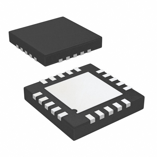
- Part No.:
- ADP8861ACPZ-RL
- Manufacturer:
- Analog Devices Inc.
- Category:
- LED Drivers
- Package:
- 20-WFQFN Exposed Pad, CSP
- Datasheet:
-
 ADP8861ACPZ-RL.pdf
- Description:
- IC LED DRV RGLTR I2C 20LFCSP
- Quantity:
- Payment:

- Shipping:

Inventory:3,755
Please send an inquiry. Send us your inquiry, and we will respond immediately.
Product details
Overview
ADP8861ACPZ-RL from Analog Devices is a 7-channel smart LED driver IC with integrated charge pump, I²C interface, and independent programmable current sinks-supporting up to six 30 mA LEDs and one 60 mA LED (D7), with automatic 1×/1.5×/2× gain selection for efficiency optimization in mobile backlighting applications.
For engineers reviewing the ADP8861ACPZ-RL datasheet, ADP8861ACPZ-RL pinout, ADP8861ACPZ-RL application, or ADP8861ACPZ-RL equivalent, key selection criteria include its 20-lead LFCSP package, 2.5 V to 5.5 V input range, <1 μA standby current, 16-step fade timing (0.1–5.5 s), and short-circuit/overvoltage/overtemperature protection for robust small-display LED control.
Technical Context
The ADP8861ACPZ-RL implements a two-capacitor switched-capacitor charge pump with automatic gain switching based on real-time current sink headroom voltage (VHR ≥ 180 mV typical); gain transitions occur only after 100 μs stabilization delay and are restricted to active LED channels.
Its I²C-compatible digital control supports full register programming of per-LED current (128 levels), fade profiles (linear/square/cubic), group dimming, and interrupt-driven fault reporting via nINT, while hardware reset (nRST) and power-on reset ensure deterministic initialization.
Key Specifications
| Parameter | Value and Actual Design Meaning |
|---|---|
| Input Voltage Range | 2.5 V to 5.5 V - supports single-cell Li-ion and Li-poly battery operation without external LDO. |
| Max Output Current | 240 mA total - enables simultaneous drive of 7 LEDs at up to 30 mA each, or D7 at 60 mA with others at 30 mA. |
| Charge Pump Gains | 1×, 1.5×, 2× - auto-selected to maintain ≥180 mV headroom across active current sinks, minimizing power loss. |
| Standby Current | <1 μA - achieved by disabling all analog circuitry except I²C receivers, critical for battery longevity. |
| Fade Timing Range | 0.1 s to 5.5 s - 16 programmable steps with selectable linear/square/cubic ramp laws for smooth visual transitions. |
| I²C Interface Speed | 400 kHz - standard Fast Mode compatible with most microcontrollers; includes noise-filtered nRST and open-drain nINT. |
| Protection Features | Short-circuit, overvoltage (5.8 V OVP), overtemperature (150 °C shutdown), and input-to-output isolation during faults. |
Pinout & Package
ADP8861ACPZ-RL is packaged in a 20-lead, 4 mm × 4 mm × 0.75 mm lead frame chip scale package (LFCSP) with exposed paddle thermally and electrically connected to GND1/GND2.
| Pin/Terminal | Circuit Role | Design Meaning |
|---|---|---|
| VIN | Power Input | Primary supply input (2.5–5.5 V); powers internal logic and charge pump. |
| VOUT | Charge Pump Output | Regulated boosted output (up to ~5.5 V); supplies all LED current sinks. |
| D1–D7 | LED Sink Outputs | Seven independent NMOS current sinks; D7 supports dual-range (30/60 mA) operation. |
| nRST | Hardware Reset | Active-low asynchronous reset with 50 μs noise filter; forces registers to default and enters standby. |
| nINT | Interrupt Output | Open-drain active-low flag signaling fault conditions (OVP, OTP, short-circuit) or fade completion. |
| SCL/SDA | I²C Interface | Standard bidirectional clock/data lines; require external pull-ups to VDDIO (≤5.5 V). |
| C1+/C1−/C2+/C2− | Charge Pump Capacitors | External flying capacitor connections; C1 and C2 each 1 μF ceramic required for stable operation. |
| GND1/GND2 | Ground Terminals | Dual ground pins; exposed paddle must be soldered to both for thermal and electrical integrity. |
Key Features
| Feature | Design Value |
|---|---|
| Auto Gain Selection | Switches between 1×, 1.5×, and 2× charge pump gains in real time to maintain ≥180 mV current sink headroom-maximizing efficiency without manual configuration. |
| Independent Sink Control | Each of seven LED channels has dedicated current programming (128 levels), fade timing, and enable/disable-enabling mixed-brightness backlighting and indicator sequencing. |
| Fade Override Capability | Allows immediate transition to target brightness level (e.g., instant on/off) bypassing programmed fade ramps-critical for user interface responsiveness. |
| Integrated Soft Start | Limiting inrush current to 3.75 mA typical during startup, restart, or gain transitions-prevents system rail droop and extends capacitor lifetime. |
| Input-to-Output Isolation | Physically disconnects VOUT from VIN during fault or shutdown-eliminates reverse current paths and protects downstream LEDs and PCB traces. |
Applications
| Mobile Display Backlighting | Mobile Keypad Backlighting |
|---|---|
Use Scenario: Driving white LEDs behind TFT-LCD panels in smartphones and portable media players with dynamic brightness control. IC Role / Device Role / Timing Role: Charge pump LED driver providing regulated current to 4–6 parallel LEDs, synchronized to display refresh rate via I²C commands. Use Value: Enables uniform, flicker-free illumination across varying battery voltages (2.5–5.5 V) while maintaining <1 μA quiescent draw during screen-off states. |
Use Scenario: Illuminating alphanumeric keypads and function buttons in feature phones and rugged handheld devices. IC Role / Device Role / Timing Role: Independent sink control allows per-key dimming and animated lighting effects using fade-in/fade-out timers. Use Value: Reduces MCU GPIO count and firmware overhead by offloading LED timing and current regulation to the ADP8861ACPZ-RL. |
| Dual RGB Indicator Lighting | Small-Format OLED Display Bias |
Use Scenario: Driving red/green/blue status indicators with color-mixing capability in networking equipment and industrial HMIs. IC Role / Device Role / Timing Role: Three dedicated sinks (e.g., D1–D3) configured for precise current matching (<2.0% mismatch) to ensure consistent chromaticity. Use Value: Eliminates need for external current-setting resistors and enables software-tuned color balance via I²C register writes. |
Use Scenario: Providing stable bias current to OLED pixel arrays in wearables and smartwatches where space and power are constrained. IC Role / Device Role / Timing Role: High-accuracy current sinks (±1.5% matching for D2–D7) deliver repeatable luminance across temperature (−40°C to +85°C). Use Value: Compensates for OLED forward voltage drift with adaptive charge pump gain-maintaining constant brightness without closed-loop sensing. |
Equivalent & Alternatives
The following parts are listed as comparable options for similar smart LED driver applications.
| Alternative Part | Technical Difference | Application Difference | Selection Advice |
|---|---|---|---|
| LM3530TMX/NOPB | 6-channel I²C LED driver; no 60 mA channel; fixed 1.5×/2× gain; no fade override; 16-pin WQFN. | Lacks D7 high-current capability and fade override-unsuitable for asymmetric backlight + indicator combos. | Select when only six uniform LEDs are needed and board space favors smaller 16-pin package. |
| MAX16984ATL+T | 8-channel driver with 30 mA max per channel; integrated boost converter (not charge pump); higher IQ (12 μA standby); 24-pin TQFN. | Higher integration but larger footprint and less efficient at low VIN; requires external inductor. | Prefer for systems requiring >240 mA total or where inductor-based boost is already present in BOM. |
Compared with LM3530TMX/NOPB and MAX16984ATL+T, the ADP8861ACPZ-RL uniquely combines 7-channel flexibility, dual-range D7 current, charge-pump efficiency below 3 V, and sub-μA standby-making it optimal for compact, battery-sensitive multi-LED systems where layout area and quiescent power are critical.
Availability
ADP8861ACPZ-RL is available at Aetrix Electronics and suitable for mobile display backlighting, keypad illumination, dual RGB indication, and small-format OLED bias applications requiring stable component supply, long-term lifecycle support, and guaranteed traceable sourcing.
Supply support for ADP8861ACPZ-RL includes scheduled delivery planning, volume procurement assistance, BOM continuity management, traceable sourcing, and lifecycle availability coordination for OEM customers, industrial embedded developers, connected-device designers, and electronics production programs.
Manufacturer
Analog Devices, Inc. is a global leader in high-performance analog, mixed-signal, and digital signal processing semiconductors, headquartered in Norwood, MA, with design and manufacturing expertise spanning precision power management and sensor signal chains.
The ADP8861ACPZ-RL belongs to Analog Devices' Smart LED Driver product line-designed specifically for ultra-low-power, highly integrated backlight and indicator control in space-constrained portable electronics.
FAQ
What is the maximum total output current supported by the ADP8861ACPZ-RL?
The ADP8861ACPZ-RL supports a maximum total output current of 240 mA. This is achieved with six LED channels (D1–D6) each delivering up to 30 mA and the seventh channel (D7) configurable for either 30 mA or 60 mA. The device dynamically manages charge pump gain and thermal limits to sustain this output across its 2.5 V to 5.5 V input range without exceeding junction temperature specifications.
Does the ADP8861ACPZ-RL require external components for basic operation?
Yes, the ADP8861ACPZ-RL requires four external ceramic capacitors: one 1 μF input capacitor (CIN), one 1 μF output capacitor (COUT), and two 1 μF flying capacitors (C1 and C2) connected to C1+/C1− and C2+/C2− pins. Additionally, pull-up resistors on SCL and SDA lines are mandatory for I²C communication, and the exposed paddle must be soldered to GND1/GND2 for thermal and electrical stability.
How does automatic gain selection work in the ADP8861ACPZ-RL?
Automatic gain selection in the ADP8861ACPZ-RL monitors the minimum voltage headroom (VHR) across all *active* LED current sinks. If VHR falls below ~200 mV, the charge pump transitions from 1× to 1.5× gain after a 100 μs stabilization delay; if insufficient, it advances to 2×. Conversely, if headroom exceeds the calculated VDMAX threshold, gain steps down to improve efficiency-ensuring optimal voltage overhead without manual intervention.
Can the ADP8861ACPZ-RL drive LEDs with different forward voltages simultaneously?
Yes, the ADP8861ACPZ-RL can drive LEDs with differing forward voltages (e.g., red, green, blue) simultaneously because each of the seven current sinks operates independently with its own compliance voltage requirement. The charge pump automatically adjusts its output voltage (VOUT) to satisfy the highest headroom demand among active sinks, while maintaining precise current regulation across all channels within ±2.0% matching tolerance.
What protection features are integrated into the ADP8861ACPZ-RL?
The ADP8861ACPZ-RL integrates short-circuit protection (triggered at VOUT < 0.55 × VIN), overvoltage protection (5.8 V threshold with 500 mV hysteresis), overtemperature shutdown (150 °C with 20 °C hysteresis), and input-to-output isolation during faults. It also includes UVLO (2.05 V start-up), soft-start current limiting (3.75 mA typical), and ESD protection rated at ±3 kV HBM-ensuring robust operation in noisy, battery-powered environments.
ADP8861ACPZ-RL Specifications
- Product attributes
- Attribute value
- Manufacturer:
- Analog Devices Inc.
- Series:
- -
- Package/Case:
- 20-WFQFN Exposed Pad, CSP
- Packaging:
- Tape & Reel (TR)
- Product Status:
- Obsolete
- Type:
- DC DC Regulator
- Topology:
- Switched Capacitor (Charge Pump)
- Internal Switch(s):
- Yes
- Number of Outputs:
- 7
- Voltage - Supply (Min):
- 2.5V
- Voltage - Supply (Max):
- 5.5V
- Voltage - Output:
- 4.3V ~ 5.5V
- Current - Output / Channel:
- 30mA, 60mA
- Frequency:
- 1MHz
- Dimming:
- I2C
- Applications:
- Backlight
- Operating Temperature:
- -40°C ~ 85°C (TA)
- Grade:
- -
- Qualification:
- -
- Mounting Type:
- Surface Mount
- Supplier Device Package:
- 20-LFCSP (4x4)
ADP8861ACPZ-RL FAQ
1.How can I place an order for ADP8861ACPZ-RL through Aetrix?
Please submit a Request for Quotation (RFQ) for ADP8861ACPZ-RL on Aetrix. Our sales agent will provide a competitive quotation and guide you through the order confirmation once you accept the terms.
2.Are the price and stock information for ADP8861ACPZ-RL reliable?
The price and inventory of ADP8861ACPZ-RL are updated periodically and may fluctuate due to market conditions. Stock and pricing data are typically refreshed every 24 hours. Quotation validity for ADP8861ACPZ-RL is usually 5 days.
3.What payment methods are accepted for ADP8861ACPZ-RL?
We accept Wire Transfer, PayPal, Credit Card, Western Union, MoneyGram, and Escrow for ADP8861ACPZ-RL transactions.
Note: Certain payment methods may incur a processing fee.
4.How is shipping managed for ADP8861ACPZ-RL?
ADP8861ACPZ-RL orders can be shipped via leading logistics carriers, including DHL, UPS, FedEx, TNT, or Registered Mail.
Once your ADP8861ACPZ-RL order is processed, you will receive an email with the shipment details and tracking number.
Note: Tracking information may take up to 24 hours to appear. Express delivery typically takes 3–5 business days.
5.How can I obtain technical support or documentation for ADP8861ACPZ-RL?
For technical support, including ADP8861ACPZ-RL datasheets, pinout diagrams, or application guidance, please contact our engineering support team. They can provide detailed documentation and assistance for your ADP8861ACPZ-RL requirements.
6.How does Aetrix verify that ADP8861ACPZ-RL is sourced from the original manufacturer or authorized distributors?
All ADP8861ACPZ-RL products on Aetrix are procured from qualified distributors and authorized channels. Our dedicated quality assurance team conducts strict verification, including traceability checks and, if necessary, third-party testing. This ensures that ADP8861ACPZ-RL meets industry standards.
7.What is the process for return or replacement of ADP8861ACPZ-RL?
All ADP8861ACPZ-RL units undergo pre-shipment inspection (PSI). If there is an issue with ADP8861ACPZ-RL, returns or replacements are accepted under the following conditions:
1.Quantity discrepancies, incorrect items, or visible external defects (such as breakage or corrosion), acknowledged by Aetrix.
2.The issue is reported within 90 days of delivery.
3.The ADP8861ACPZ-RL part is unused and in its original packaging.
Return procedure for ADP8861ACPZ-RL:
1.Submit a request within 90 days.
2.Obtain a Return Material Authorization (RMA) from Aetrix.
ADP8861ACPZ-RL Tags

-
BCR402RE6327HTSA1
Infineon Technologies

-
BCR430UXTSA2
Infineon Technologies

-
BCR420UE6433HTMA1
Infineon Technologies
-
BCR420UE6327HTSA1
Infineon Technologies
-
BCR421UE6327HTSA1
Infineon Technologies

-
LYT1604D-TL
Power Integrations

-
HV9910CLG-G
Microchip Technology

-
CL2N8-G
Microchip Technology

-
BCR420UW6-7
Diodes Incorporated
-
BCR421UW6-7
Diodes Incorporated

-
BCR420UFD-7
Diodes Incorporated
-
BCR421UFD-7
Diodes Incorporated
Tech Hub

A practical engineering guide to 3.3V and 5V logic compatibility, input thresholds, resistor dividers, translator ICs, MOSFET level shifting, I2C pull-ups, timing limits and power-sequencing risks.

The 74HC595 uses push-pull logic outputs, while the TPIC6B595 uses 50 V open-drain DMOS sinks for higher-power loads. This guide compares timing, current limits, 3.3 V interfacing, load wiring, thermal…

The 74HC595 converts serial data into eight stable parallel outputs. This guide covers pin functions, shift and storage timing, OE and MR behavior, drive-current limits, cascading, voltage compatibilit…

A technical comparison of level-sensitive latches and edge-triggered flip-flops, covering timing windows, setup and hold limits, master–slave operation, time borrowing, race-through, HDL inference and…

A D latch stores one bit while Enable controls when data can pass. This reference covers gate-level operation, truth tables, transparency, setup and hold timing, LE versus OE, common ICs and practical …

An SR latch stores one bit through cross-coupled feedback. This engineering reference covers NOR and NAND implementations, truth tables, forbidden-state recovery, gated operation, switch debouncing, fa…

Latch circuits retain one bit through feedback. This technical reference covers SR and D latches, truth tables, transparency, timing limits, latch-versus-flip-flop behavior, applications and common log…

An engineering guide to LED driver operation, constant-current and constant-voltage outputs, linear and switching topologies, dimming, IC selection, calculations, replacement compatibility, and fault c…

Operational amplifier guide covering op amp basics, feedback, ideal vs real op amps, common configurations, buffer circuits, offset, bias current, gain-bandwidth, slew rate, rail-to-rail limits and sel…

Jumper cables guide covering safe connection order, red and black clamp placement, final ground connection, cable gauge, length, clamp quality, copper vs CCA cables, jump starter comparison and battery…


