
 My Inquiry
 My Account


Analog Devices Inc. ADP8863ACPZ-R7
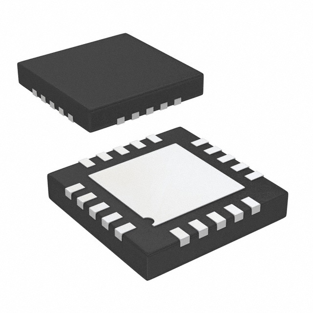
- Part No.:
- ADP8863ACPZ-R7
- Manufacturer:
- Analog Devices Inc.
- Category:
- LED Drivers
- Package:
- 20-WFQFN Exposed Pad, CSP
- Datasheet:
-
 ADP8863ACPZ-R7.pdf
- Description:
- IC LED DRV RGLTR I2C 20LFCSP
- Quantity:
- Payment:

- Shipping:

Inventory:1,607
Please send an inquiry. Send us your inquiry, and we will respond immediately.
Product details
Overview
ADP8863ACPZ-R7 from Analog Devices is a 7-channel autonomous LED charge pump driver IC designed for fun lighting, keypad backlighting, and RGB color mixing in portable electronics. It delivers up to 30 mA per channel (D1–D6) and 60 mA on D7, features I²C-programmable fade timing (0.1–5.5 s), automatic gain selection (1×/1.5×/2×), and integrated ambient light sensing via two comparator inputs.
For engineers reviewing the ADP8863ACPZ-R7 datasheet, ADP8863ACPZ-R7 pinout, ADP8863ACPZ-R7 application, or ADP8863ACPZ-R7 equivalent, key selection considerations include its WLCSP/LFCSP package options, 2.5 V to 5.5 V input range, <1 μA standby current, short-circuit/overvoltage/overtemperature protection, and independent sink control with 128-level current programming.
Technical Context
The ADP8863ACPZ-R7 integrates a dual-capacitor charge pump with automatic gain switching among 1×, 1.5×, and 2× modes based on real-time LED sink headroom voltage (VHR), ensuring optimal efficiency across varying forward voltages and supply conditions. Its internal soft-start limits inrush current to 3.75 mA typical during startup and gain transitions.
It supports autonomous LED operation via programmable fade-in/fade-out (16 settings, linear/square/cubic profiles), independent blinking per channel, and group-based backlight control. The I²C interface (400 kHz, 2.7 V logic) enables full register access for current, timing, comparator thresholds, and fault management - all while maintaining <1 μA quiescent current in standby mode.
Key Specifications
| Parameter | Value and Actual Design Meaning |
|---|---|
| Input Voltage Range | 2.5 V to 5.5 V - supports single-cell Li-ion and Li-poly battery systems without external regulation. |
| Max Output Current | 240 mA total - enables simultaneous drive of seven LEDs at full brightness (e.g., six at 30 mA + one at 60 mA). |
| LED Sink Current | D1–D6: 30 mA max; D7: 60 mA max - allows high-brightness indicator or RGB primary channel with enhanced current capability. |
| Fade Timing Range | 0.1 s to 5.5 s - provides precise visual effects for user interface feedback and dynamic lighting sequences. |
| Charge Pump Gains | 1×, 1.5×, 2× - automatically selected to maintain ≥200 mV sink headroom while minimizing power loss. |
| Standby Current | <1 μA - enables ultra-low-power retention in always-on or wake-on-event mobile applications. |
| Ambient Light Sensing | Two programmable comparator inputs - supports closed-loop display backlight dimming using phototransistor or photodiode sensors. |
Pinout & Package
ADP8863ACPZ-R7 is available in a 20-ball, 2.15 mm × 2.36 mm × 0.6 mm WLCSP (Wafer Level Chip Scale Package) with exposed paddle connected to GND1/GND2. Pin functions are ball-mapped as shown below:
| Pin/Terminal | Circuit Role | Design Meaning |
|---|---|---|
| VIN | Power Input | 2.5 V–5.5 V main supply; feeds charge pump and internal logic; includes UVLO (2.05 V start-up). |
| VOUT | Charge Pump Output | Regulated boosted output (up to 5.5 V); powers all seven LED sinks; isolated during faults. |
| D1–D7 | LED Sink Outputs | Seven independent current-sink terminals; D7 supports dual-mode (30 mA or 60 mA); each programmable via I²C. |
| C1+, C1−, C2+, C2− | Charge Pump Capacitor Terminals | Interface for two external 1 μF ceramic capacitors; defines charge pump topology and gain behavior. |
| SCL / SDA | I²C Interface | Standard 400 kHz I²C bus; supports full register read/write for LED timing, current, fade, and sensor configuration. |
| nRST / nINT | Reset & Interrupt | Active-low hardware reset with 50 μs noise filter; open-drain interrupt output signals fault or fade completion. |
| CMP_IN | Ambient Light Sensor Input | Comparator input for phototransistor; requires 0.1 μF decoupling capacitor to GND for stable ALS operation. |
Key Features
| Feature | Design Value |
|---|---|
| Autonomous Fade Control | 16 programmable fade-in/fade-out times (0.1–5.5 s) with selectable linear/square/cubic profiles - eliminates MCU intervention for smooth LED transitions. |
| Intelligent Gain Selection | Real-time 1×/1.5×/2× charge pump gain switching based on minimum LED sink headroom voltage - maximizes efficiency without manual gain scheduling. |
| RGB Color Mixing Support | Independent current and timing control per channel (D1–D7) - enables precise hue/saturation adjustment and automated color fades for UI indicators. |
| Integrated Light Sensing | Two comparator inputs with programmable thresholds (L2/L3) - allows adaptive backlight dimming using off-the-shelf ambient light sensors. |
| Fault Protection Suite | Short-circuit, overvoltage (5.8 V OVP), overtemperature (150 °C shutdown), and input-to-output isolation - ensures robust operation in unattended portable systems. |
Applications
| Keypad Backlighting | RGB LED Color Generation |
|---|---|
|
Use Scenario: Illuminating alphanumeric keypads in smartphones, wearables, and industrial handhelds under variable ambient light. IC Role / Device Role / Timing Role: Autonomous backlight controller managing D1–D6 as uniform white-light sources with programmable fade-on/off and ambient-adaptive dimming. Use Value: Reduces host processor load by executing fade sequences independently; extends battery life via <1 μA standby current and efficient charge pump gain selection. |
Use Scenario: Generating dynamic color themes and status indicators using red/green/blue LEDs in consumer electronics UIs. IC Role / Device Role / Timing Role: Independent current sink driver for R/G/B channels (e.g., D1=R, D2=G, D3=B) with synchronized fade timing and 128-level intensity resolution. Use Value: Enables smooth, flicker-free color transitions without MCU timing overhead; supports cubic fade for perceptually uniform brightness ramps. |
| Funlight Indicator Lighting | Small-Format Display Backlighting |
|
Use Scenario: Creating attention-grabbing visual effects (blinking, pulsing, breathing) on device edges or status rings in IoT sensors and smart accessories. IC Role / Device Role / Timing Role: Autonomous LED sequencer driving D1–D7 with independent blink patterns, fade rates, and group enable/disable via I²C registers. Use Value: Eliminates need for dedicated LED animation firmware; supports 16 distinct fade durations and three fade curve types for rich visual differentiation. |
Use Scenario: Powering edge-lit or direct-backlit monochrome or color TFT displays in portable medical devices and instrumentation panels. IC Role / Device Role / Timing Role: High-efficiency charge pump driver delivering regulated VOUT to multiple parallel LED strings (e.g., D4–D7 as backlight bank) with thermal-aware current limiting. Use Value: Maintains consistent brightness across 2.5–5.5 V input range; prevents thermal runaway via overtemperature shutdown and current matching ≤2.0% across sinks. |
Equivalent & Alternatives
The following parts are listed as comparable options for similar LED driver applications.
| Alternative Part | Technical Difference | Application Difference | Selection Advice |
|---|---|---|---|
| IS31FL3728-QFLS4-TR | 4×4 matrix LED driver with PWM dimming; no charge pump; requires external boost or bias supply. | Designed for grid-addressed LED arrays; lacks autonomous fade, ambient sensing, and charge pump integration. | Choose when driving multiplexed LED matrices rather than discrete sinks; not suitable for single-supply 2.5 V battery operation. |
| TPS61165DRVR | Single-channel 40 V boost LED driver with analog/digital dimming; no I²C, no multi-channel autonomy. | Optimized for high-Vf white LEDs in flash or display backlight; no fade timing, group control, or ALS support. | Choose for high-current single-LED applications (e.g., camera flash); requires external MCU for sequencing and sensing logic. |
Compared with IS31FL3728-QFLS4-TR and TPS61165DRVR, the ADP8863ACPZ-R7 uniquely combines 7-channel autonomous sink control, integrated charge pump, ambient light sensing, and programmable fade in a single compact package - making it optimal for battery-powered UI lighting where MCU offload and power efficiency are critical.
Availability
ADP8863ACPZ-R7 is available at Aetrix Electronics and suitable for keypad backlighting, RGB LED color generation, funlight indicator lighting, small-format display backlighting, and ambient-adaptive UI lighting requiring stable component supply and long-term production continuity.
Supply support for ADP8863ACPZ-R7 includes scheduled delivery planning, volume procurement assistance, BOM continuity management, traceable sourcing, and lifecycle availability coordination for OEM customers, industrial embedded developers, connected-device designers, and electronics production programs.
Manufacturer
Analog Devices is a global leader in high-performance analog, mixed-signal, and digital signal processing semiconductors, serving industrial, automotive, communications, and consumer markets with precision power, sensing, and interface solutions.
The ADP8863ACPZ-R7 belongs to Analog Devices' autonomous LED driver product line, engineered specifically for low-power, visually engaging user interfaces in space-constrained portable electronics - emphasizing MCU offload, battery longevity, and seamless ambient adaptation.
FAQ
What is the maximum LED forward voltage supported by ADP8863ACPZ-R7?
The ADP8863ACPZ-R7 supports LED forward voltages up to 4.1 V when operating in 30 mA mode (D1–D6) and maintains regulation up to 4.25 V in 60 mA mode (D7), enabled by its 2× charge pump gain delivering up to 5.5 V regulated VOUT. This accommodates standard white, red, green, and blue LEDs across battery voltage ranges from 2.5 V to 5.5 V.
Does ADP8863ACPZ-R7 require external components for basic operation?
Yes, ADP8863ACPZ-R7 requires four external ceramic capacitors: one 1 μF input capacitor (CIN), one 1 μF output capacitor (COUT), and two 1 μF charge pump capacitors (C1, C2). A 0.1 μF capacitor is also required on CMP_IN if ambient light sensing is used. No external inductors or resistors are needed for core LED driving functionality.
How does the automatic gain selection work in ADP8863ACPZ-R7?
ADP8863ACPZ-R7 monitors the minimum voltage across all active LED sinks (VD1–VD7) and switches charge pump gain (1× → 1.5× → 2×) when headroom falls below ~200 mV. After each gain change, a 100 μs stabilization delay occurs before re-evaluation. Gain reduces when headroom exceeds VDMAX - an internally calculated threshold ensuring sufficient margin at lower gain.
Can ADP8863ACPZ-R7 drive more than seven LEDs?
No, ADP8863ACPZ-R7 has exactly seven dedicated current-sink outputs (D1–D7). However, multiple ADP8863ACPZ-R7 devices can be cascaded or synchronized via I²C to control larger LED arrays. Each device retains independent fade, current, and timing control - enabling scalable lighting systems without increasing MCU complexity.
What protection features does ADP8863ACPZ-R7 include?
ADP8863ACPZ-R7 includes short-circuit protection (VOUT drops to 0.55 × VIN), overvoltage protection (5.8 V threshold with 500 mV hysteresis), overtemperature shutdown (150 °C with 20 °C hysteresis), input-to-output isolation during faults, and internal soft-start to limit inrush current. All protections trigger automatic recovery or require explicit reset - ensuring safe, maintenance-free operation.
ADP8863ACPZ-R7 Specifications
- Product attributes
- Attribute value
- Manufacturer:
- Analog Devices Inc.
- Series:
- -
- Package/Case:
- 20-WFQFN Exposed Pad, CSP
- Packaging:
- Tape & Reel (TR)
- Product Status:
- Active
- Type:
- DC DC Regulator
- Topology:
- Switched Capacitor (Charge Pump)
- Internal Switch(s):
- Yes
- Number of Outputs:
- 7
- Voltage - Supply (Min):
- 2.5V
- Voltage - Supply (Max):
- 5.5V
- Voltage - Output:
- 4.3V ~ 5.5V
- Current - Output / Channel:
- 30mA, 60mA
- Frequency:
- 1MHz
- Dimming:
- I2C
- Applications:
- Backlight
- Operating Temperature:
- -40°C ~ 85°C (TA)
- Grade:
- -
- Qualification:
- -
- Mounting Type:
- Surface Mount
- Supplier Device Package:
- 20-LFCSP (4x4)
ADP8863ACPZ-R7 FAQ
1.How can I place an order for ADP8863ACPZ-R7 through Aetrix?
Please submit a Request for Quotation (RFQ) for ADP8863ACPZ-R7 on Aetrix. Our sales agent will provide a competitive quotation and guide you through the order confirmation once you accept the terms.
2.Are the price and stock information for ADP8863ACPZ-R7 reliable?
The price and inventory of ADP8863ACPZ-R7 are updated periodically and may fluctuate due to market conditions. Stock and pricing data are typically refreshed every 24 hours. Quotation validity for ADP8863ACPZ-R7 is usually 5 days.
3.What payment methods are accepted for ADP8863ACPZ-R7?
We accept Wire Transfer, PayPal, Credit Card, Western Union, MoneyGram, and Escrow for ADP8863ACPZ-R7 transactions.
Note: Certain payment methods may incur a processing fee.
4.How is shipping managed for ADP8863ACPZ-R7?
ADP8863ACPZ-R7 orders can be shipped via leading logistics carriers, including DHL, UPS, FedEx, TNT, or Registered Mail.
Once your ADP8863ACPZ-R7 order is processed, you will receive an email with the shipment details and tracking number.
Note: Tracking information may take up to 24 hours to appear. Express delivery typically takes 3–5 business days.
5.How can I obtain technical support or documentation for ADP8863ACPZ-R7?
For technical support, including ADP8863ACPZ-R7 datasheets, pinout diagrams, or application guidance, please contact our engineering support team. They can provide detailed documentation and assistance for your ADP8863ACPZ-R7 requirements.
6.How does Aetrix verify that ADP8863ACPZ-R7 is sourced from the original manufacturer or authorized distributors?
All ADP8863ACPZ-R7 products on Aetrix are procured from qualified distributors and authorized channels. Our dedicated quality assurance team conducts strict verification, including traceability checks and, if necessary, third-party testing. This ensures that ADP8863ACPZ-R7 meets industry standards.
7.What is the process for return or replacement of ADP8863ACPZ-R7?
All ADP8863ACPZ-R7 units undergo pre-shipment inspection (PSI). If there is an issue with ADP8863ACPZ-R7, returns or replacements are accepted under the following conditions:
1.Quantity discrepancies, incorrect items, or visible external defects (such as breakage or corrosion), acknowledged by Aetrix.
2.The issue is reported within 90 days of delivery.
3.The ADP8863ACPZ-R7 part is unused and in its original packaging.
Return procedure for ADP8863ACPZ-R7:
1.Submit a request within 90 days.
2.Obtain a Return Material Authorization (RMA) from Aetrix.
ADP8863ACPZ-R7 Tags

-
BCR402RE6327HTSA1
Infineon Technologies

-
BCR430UXTSA2
Infineon Technologies

-
BCR420UE6433HTMA1
Infineon Technologies
-
BCR420UE6327HTSA1
Infineon Technologies
-
BCR421UE6327HTSA1
Infineon Technologies

-
LYT1604D-TL
Power Integrations

-
HV9910CLG-G
Microchip Technology

-
CL2N8-G
Microchip Technology

-
BCR420UW6-7
Diodes Incorporated
-
BCR421UW6-7
Diodes Incorporated

-
BCR420UFD-7
Diodes Incorporated
-
BCR421UFD-7
Diodes Incorporated
Tech Hub

A practical engineering guide to 3.3V and 5V logic compatibility, input thresholds, resistor dividers, translator ICs, MOSFET level shifting, I2C pull-ups, timing limits and power-sequencing risks.

The 74HC595 uses push-pull logic outputs, while the TPIC6B595 uses 50 V open-drain DMOS sinks for higher-power loads. This guide compares timing, current limits, 3.3 V interfacing, load wiring, thermal…

The 74HC595 converts serial data into eight stable parallel outputs. This guide covers pin functions, shift and storage timing, OE and MR behavior, drive-current limits, cascading, voltage compatibilit…

A technical comparison of level-sensitive latches and edge-triggered flip-flops, covering timing windows, setup and hold limits, master–slave operation, time borrowing, race-through, HDL inference and…

A D latch stores one bit while Enable controls when data can pass. This reference covers gate-level operation, truth tables, transparency, setup and hold timing, LE versus OE, common ICs and practical …

An SR latch stores one bit through cross-coupled feedback. This engineering reference covers NOR and NAND implementations, truth tables, forbidden-state recovery, gated operation, switch debouncing, fa…

Latch circuits retain one bit through feedback. This technical reference covers SR and D latches, truth tables, transparency, timing limits, latch-versus-flip-flop behavior, applications and common log…

An engineering guide to LED driver operation, constant-current and constant-voltage outputs, linear and switching topologies, dimming, IC selection, calculations, replacement compatibility, and fault c…

Operational amplifier guide covering op amp basics, feedback, ideal vs real op amps, common configurations, buffer circuits, offset, bias current, gain-bandwidth, slew rate, rail-to-rail limits and sel…

Jumper cables guide covering safe connection order, red and black clamp placement, final ground connection, cable gauge, length, clamp quality, copper vs CCA cables, jump starter comparison and battery…


