
 My Inquiry
 My Account


Analog Devices Inc. ADP8870ACPZ-R7
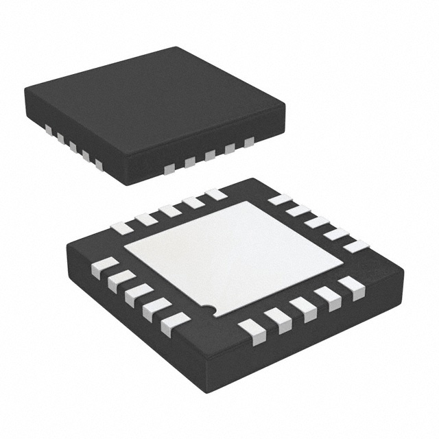
- Part No.:
- ADP8870ACPZ-R7
- Manufacturer:
- Analog Devices Inc.
- Category:
- LED Drivers
- Package:
- 20-WFQFN Exposed Pad, CSP
- Datasheet:
-
 ADP8870ACPZ-R7.pdf
- Description:
- IC LED DRV RGLTR PWM 20LFCSP
- Quantity:
- Payment:

- Shipping:

Inventory:2,224
Please send an inquiry. Send us your inquiry, and we will respond immediately.
Product details
Overview
ADP8870ACPZ-R7 from Analog Devices is a programmable 7-channel LED charge-pump backlight driver with integrated ambient light sensing (ALS), image-content-adaptive PWM dimming, and automatic gain selection (1×/1.5×/2×). It delivers up to 6 × 30 mA + 1 × 60 mA sink current, operates from 2.5 V to 5.5 V input, supports I²C programming, and features <1 μA standby current. It targets mobile display and keypad backlighting where power efficiency and autonomous brightness control are critical.
For engineers reviewing the ADP8870ACPZ-R7 datasheet, ADP8870ACPZ-R7 pinout, ADP8870ACPZ-R7 application, or ADP8870ACPZ-R7 equivalent, this page provides verified technical context, real-world design meaning for key specs, validated package and pin mapping, confirmed alternative options, and supply-ready availability details - all grounded in the Rev. C datasheet and official Analog Devices documentation.
Technical Context
The ADP8870ACPZ-R7 integrates a dual-capacitor charge-pump with automatic gain switching (1×/1.5×/2×) based on real-time LED sink headroom voltage (VHR), enabling optimal efficiency across varying VIN and LED forward voltages. Its ALS subsystem uses two phototransistor inputs with five programmable light-sensing zones and ±5% accuracy comparators.
It accepts a dedicated PWM input for content-adaptive brightness control (CABC), scaling LED output current linearly (±1.4% deviation) across 140 Hz–60 kHz frequency range. All seven LED channels are independently programmable for current (128-level DAC), fade timing (16 presets), and group behavior via I²C interface - eliminating processor intervention for ambient- and content-driven dimming.
Key Specifications
| Parameter | Value and Actual Design Meaning |
|---|---|
| Input Voltage Range | 2.5 V to 5.5 V - supports single-cell Li-ion and Li-poly battery systems without external LDO. |
| LED Drive Capability | 6 × 30 mA + 1 × 60 mA sinks - enables full-color RGB backlight or high-brightness keypad illumination with one device. |
| Charge-Pump Gains | 1×, 1.5×, 2× auto-selected - maintains regulation headroom while minimizing quiescent current (e.g., IQ = 1.4 mA at 1×, 3.9 mA at 1.5×). |
| Ambient Light Sensing | Two ±5% accurate phototransistor inputs with 5-zone programmability - enables precise, multi-threshold ambient adaptation without MCU polling. |
| PWM Input Support | 140 Hz–60 kHz, ±1.0% accuracy at 50% duty cycle - directly scales LED current for CABC, reducing display power by up to 40% in dark-content scenes. |
| Standby Current | <1 μA - preserves battery life during screen-off states in portable devices. |
| I²C Interface | Standard-mode (400 kHz), 3.6 V logic compatible - allows seamless integration with ARM Cortex-M or application processors. |
Pinout & Package
ADP8870ACPZ-R7 is available in a lead frame chip scale package (LFCSP), 4 mm × 4 mm × 0.75 mm, with exposed paddle requiring GND connection for thermal and electrical integrity.
| Pin/Terminal | Circuit Role | Design Meaning |
|---|---|---|
| VIN | Power Input | Main supply input (2.5 V–5.5 V); powers internal regulators and charge pump. |
| VOUT | Charge-Pump Output | Regulated boosted output driving all LED anodes; voltage dynamically adjusted per gain mode. |
| GND | Ground Reference | Common return for power, logic, and LED sinks; exposed paddle must be soldered to GND plane. |
| D1–D6 | LED Sink Outputs | Independent 30 mA max current sinks; each drives one LED cathode with programmable current/fade. |
| D7 | High-Current LED Sink | 60 mA max sink - used for keypad backlight or high-intensity indicator; supports independent ALS control. |
| CMP_IN | Phototransistor Comparator Input | First ALS input; requires 0.1 µF capacitor to GND for noise filtering and stable threshold detection. |
| D6 (alt) | Secondary Phototransistor Input | Second ALS input when configured via register; enables dual-zone ambient sensing for wider dynamic range. |
| PWM | Image-Content Dimming Input | Direct analog-scale control of LED current; enables CABC without MCU firmware overhead. |
| SCL / SDA | I²C Interface | Standard bidirectional bus for full configuration (current, fade, ALS thresholds, gain enable). |
| nRST | Hardware Reset | Active-low asynchronous reset; holds device in standby with registers cleared until deasserted. |
| nINT | Interrupt Output | Open-drain active-low signal indicating fault (OVP, TSD, SCP) or fade completion. |
| C1+/C1−, C2+/C2− | Charge-Pump Capacitor Terminals | Connect external flying capacitors (1 µF each) - defines charge-pump topology and efficiency. |
Key Features
| Feature | Design Value |
|---|---|
| Automatic Gain Selection | Selects 1×/1.5×/2× charge-pump gain in real time based on minimum LED sink headroom voltage - sustains regulation while minimizing IQ and heat. |
| Programmable Fade Timing | 16 fade-in/fade-out durations (0.1 s–5.5 s) with square/cubic rate options - eliminates visible flicker during backlight transitions. |
| Dedicated D7 ALS Control | Independent ambient light response for keypad LEDs - enables context-aware UI lighting separate from display backlight. |
| Fault Protection Suite | Integrated short-circuit, overvoltage (5.7 V), and overtemperature (150 °C) protection with input-output isolation - ensures robust operation in unattended mobile systems. |
| Soft Start & UVLO | Controlled 7 mA start-up current and 2.02 V undervoltage lockout - prevents erratic behavior during battery brownout or cold-start conditions. |
Applications
| Mobile Display Backlighting | Mobile Keypad Backlighting |
|---|---|
Use Scenario: Backlighting small-format LCD or OLED displays in smartphones and wearables under variable ambient light and image content. IC Role / Device Role / Timing Role: Charge-pump LED driver with autonomous ALS and PWM-based CABC - regulates LED current without CPU involvement. Use Value: Reduces average display power by >30% versus fixed-brightness solutions, extending battery runtime in always-on display modes. |
Use Scenario: Illuminating alphanumeric keypads in feature phones or industrial handhelds with adaptive brightness. IC Role / Device Role / Timing Role: Dedicated D7 sink with independent ALS control - adjusts keypad intensity separately from main display. Use Value: Maintains legibility in low-light environments while avoiding glare in bright conditions - improves UX across lighting conditions. |
| RGB LED Lighting | LED Indication |
Use Scenario: Driving red/green/blue LEDs for status indication or color-tuned UI feedback in portable medical or consumer devices. IC Role / Device Role / Timing Role: 7-channel independent current sink with 128-level DAC resolution - enables precise color mixing and smooth transitions. Use Value: Eliminates need for external current-setting resistors or discrete drivers, reducing BOM count and PCB area by ≥40%. |
Use Scenario: Low-power status indicators (e.g., charging, Bluetooth, power-on) in battery-powered IoT sensors and accessories. IC Role / Device Role / Timing Role: Standby current <1 μA and programmable fade - enables persistent visual feedback without draining coin cells. Use Value: Supports >1-year operation on CR2032 batteries with periodic LED pulsing, verified per datasheet leakage specs. |
Equivalent & Alternatives
The following parts are listed as comparable options for similar LED backlight driver applications.
| Alternative Part | Technical Difference | Application Difference | Selection Advice |
|---|---|---|---|
| LM3530TMX/NOPB | 6-channel, 30 mA/channel; no D7 60 mA option; ALS only on single input; no CABC PWM input. | Lacks independent keypad control and image-content dimming - suitable only for basic display-only use cases. | Choose if system requires only 6-channel drive and no CABC; lower cost but reduced flexibility. |
| MAX16984ATL+T | 4-channel, 40 mA/channel; integrated boost converter (not charge-pump); no ALS or PWM scaling; higher IQ (2.5 mA active). | Designed for automotive infotainment; lacks ambient/content adaptation - requires external MCU control loop. | Prefer for 12 V automotive systems needing higher per-channel current; not drop-in for portable battery-powered designs. |
Compared with LM3530TMX/NOPB and MAX16984ATL+T, the ADP8870ACPZ-R7 uniquely combines 7-channel drive (including 60 mA D7), dual ALS inputs, and hardware CABC - enabling fully autonomous, power-optimized backlighting in space-constrained portable designs without MCU resource overhead.
Availability
ADP8870ACPZ-R7 is available at Aetrix Electronics and suitable for mobile display backlighting, keypad illumination, RGB lighting, LED indication, and general small-format display applications requiring stable component supply, long-term lifecycle support, and guaranteed traceable sourcing.
Supply support for ADP8870ACPZ-R7 includes scheduled delivery planning, volume procurement assistance, BOM continuity management, traceable sourcing, and lifecycle availability coordination for OEM customers, industrial embedded developers, connected-device designers, and electronics production programs.
Manufacturer
Analog Devices, Inc. is a global leader in high-performance analog, mixed-signal, and digital signal processing semiconductors, headquartered in Norwood, MA, with R&D and manufacturing operations worldwide.
The ADP8870ACPZ-R7 belongs to Analog Devices' Power Management portfolio, specifically designed for energy-efficient, intelligent LED backlighting in battery-powered portable electronics - emphasizing autonomous ambient/content adaptation and minimal MCU intervention.
FAQ
What is the primary function of the ADP8870ACPZ-R7?
The ADP8870ACPZ-R7 is a highly integrated LED backlight driver that autonomously controls brightness using ambient light sensing (ALS) and image-content-adaptive PWM dimming. It combines a 7-channel current sink (6 × 30 mA + 1 × 60 mA), auto-selecting charge-pump (1×/1.5×/2×), and I²C programmability - enabling significant power savings in mobile displays without continuous MCU supervision. Its core value lies in eliminating software-based brightness loops.
Does the ADP8870ACPZ-R7 support true content-adaptive brightness control (CABC)?
Yes, the ADP8870ACPZ-R7 supports hardware-based CABC via its dedicated PWM input pin. Unlike software-controlled alternatives, this feature directly scales LED output current in real time - with ±1.4% linearity from 100% to 25% duty cycle and sub-millisecond response - allowing dynamic backlight reduction during dark-content scenes. This capability is explicitly documented in the Rev. C datasheet Section "Image Content Control" and Figure 13–14 performance curves.
How does the automatic gain selection work in the ADP8870ACPZ-R7?
The ADP8870ACPZ-R7 monitors the minimum headroom voltage (VHR) across all active LED sinks and switches charge-pump gain (1× → 1.5× → 2×) when VHR falls below 115–245 mV, with 100 μs stabilization delay between steps. Gain reduces when VHR exceeds a calculated VD(MAX) threshold - ensuring optimal efficiency without sacrificing regulation. This behavior is defined in the "Automatic Gain Selection" section (p.13) and illustrated in Figure 28 of the Rev. C datasheet.
Can the ADP8870ACPZ-R7 drive both display and keypad LEDs independently?
Yes - the ADP8870ACPZ-R7 provides independent ALS control for D7, allowing keypad LEDs to respond to ambient light separately from the main display backlight (D1–D6). This is implemented via dedicated comparator circuitry and register-controlled thresholds, enabling context-aware UI lighting. The datasheet confirms this in "D7 Ambient Light-Sensing Control" (p.20) and "Applications" (p.1).
What package options are available for the ADP8870ACPZ-R7?
The ADP8870ACPZ-R7 is offered in a 4 mm × 4 mm × 0.75 mm lead frame chip scale package (LFCSP) with exposed thermal pad - specified in the "Ordering Guide" (p.57) and "Outline Dimensions" (p.56) of Rev. C. While the WLCSP variant exists (2.15 mm × 2.36 mm), the -R7 suffix denotes the LFCSP tape-and-reel version. Pin mapping, thermal resistance (θJA = 49.5°C/W), and soldering requirements are fully documented for this package.
ADP8870ACPZ-R7 Specifications
- Product attributes
- Attribute value
- Manufacturer:
- Analog Devices Inc.
- Series:
- -
- Package/Case:
- 20-WFQFN Exposed Pad, CSP
- Packaging:
- Tape & Reel (TR)
- Product Status:
- Active
- Type:
- DC DC Regulator
- Topology:
- Switched Capacitor (Charge Pump)
- Internal Switch(s):
- Yes
- Number of Outputs:
- 7
- Voltage - Supply (Min):
- 2.5V
- Voltage - Supply (Max):
- 5.5V
- Voltage - Output:
- -
- Current - Output / Channel:
- 30mA, 60mA
- Frequency:
- -
- Dimming:
- PWM
- Applications:
- Backlight
- Operating Temperature:
- -
- Grade:
- -
- Qualification:
- -
- Mounting Type:
- Surface Mount
- Supplier Device Package:
- 20-LFCSP (4x4)
ADP8870ACPZ-R7 FAQ
1.How can I place an order for ADP8870ACPZ-R7 through Aetrix?
Please submit a Request for Quotation (RFQ) for ADP8870ACPZ-R7 on Aetrix. Our sales agent will provide a competitive quotation and guide you through the order confirmation once you accept the terms.
2.Are the price and stock information for ADP8870ACPZ-R7 reliable?
The price and inventory of ADP8870ACPZ-R7 are updated periodically and may fluctuate due to market conditions. Stock and pricing data are typically refreshed every 24 hours. Quotation validity for ADP8870ACPZ-R7 is usually 5 days.
3.What payment methods are accepted for ADP8870ACPZ-R7?
We accept Wire Transfer, PayPal, Credit Card, Western Union, MoneyGram, and Escrow for ADP8870ACPZ-R7 transactions.
Note: Certain payment methods may incur a processing fee.
4.How is shipping managed for ADP8870ACPZ-R7?
ADP8870ACPZ-R7 orders can be shipped via leading logistics carriers, including DHL, UPS, FedEx, TNT, or Registered Mail.
Once your ADP8870ACPZ-R7 order is processed, you will receive an email with the shipment details and tracking number.
Note: Tracking information may take up to 24 hours to appear. Express delivery typically takes 3–5 business days.
5.How can I obtain technical support or documentation for ADP8870ACPZ-R7?
For technical support, including ADP8870ACPZ-R7 datasheets, pinout diagrams, or application guidance, please contact our engineering support team. They can provide detailed documentation and assistance for your ADP8870ACPZ-R7 requirements.
6.How does Aetrix verify that ADP8870ACPZ-R7 is sourced from the original manufacturer or authorized distributors?
All ADP8870ACPZ-R7 products on Aetrix are procured from qualified distributors and authorized channels. Our dedicated quality assurance team conducts strict verification, including traceability checks and, if necessary, third-party testing. This ensures that ADP8870ACPZ-R7 meets industry standards.
7.What is the process for return or replacement of ADP8870ACPZ-R7?
All ADP8870ACPZ-R7 units undergo pre-shipment inspection (PSI). If there is an issue with ADP8870ACPZ-R7, returns or replacements are accepted under the following conditions:
1.Quantity discrepancies, incorrect items, or visible external defects (such as breakage or corrosion), acknowledged by Aetrix.
2.The issue is reported within 90 days of delivery.
3.The ADP8870ACPZ-R7 part is unused and in its original packaging.
Return procedure for ADP8870ACPZ-R7:
1.Submit a request within 90 days.
2.Obtain a Return Material Authorization (RMA) from Aetrix.
ADP8870ACPZ-R7 Tags

-
BCR402RE6327HTSA1
Infineon Technologies

-
BCR430UXTSA2
Infineon Technologies

-
BCR420UE6433HTMA1
Infineon Technologies
-
BCR420UE6327HTSA1
Infineon Technologies
-
BCR421UE6327HTSA1
Infineon Technologies

-
LYT1604D-TL
Power Integrations

-
HV9910CLG-G
Microchip Technology

-
CL2N8-G
Microchip Technology

-
BCR420UW6-7
Diodes Incorporated
-
BCR421UW6-7
Diodes Incorporated

-
BCR420UFD-7
Diodes Incorporated
-
BCR421UFD-7
Diodes Incorporated
Tech Hub

A practical engineering guide to 3.3V and 5V logic compatibility, input thresholds, resistor dividers, translator ICs, MOSFET level shifting, I2C pull-ups, timing limits and power-sequencing risks.

The 74HC595 uses push-pull logic outputs, while the TPIC6B595 uses 50 V open-drain DMOS sinks for higher-power loads. This guide compares timing, current limits, 3.3 V interfacing, load wiring, thermal…

The 74HC595 converts serial data into eight stable parallel outputs. This guide covers pin functions, shift and storage timing, OE and MR behavior, drive-current limits, cascading, voltage compatibilit…

A technical comparison of level-sensitive latches and edge-triggered flip-flops, covering timing windows, setup and hold limits, master–slave operation, time borrowing, race-through, HDL inference and…

A D latch stores one bit while Enable controls when data can pass. This reference covers gate-level operation, truth tables, transparency, setup and hold timing, LE versus OE, common ICs and practical …

An SR latch stores one bit through cross-coupled feedback. This engineering reference covers NOR and NAND implementations, truth tables, forbidden-state recovery, gated operation, switch debouncing, fa…

Latch circuits retain one bit through feedback. This technical reference covers SR and D latches, truth tables, transparency, timing limits, latch-versus-flip-flop behavior, applications and common log…

An engineering guide to LED driver operation, constant-current and constant-voltage outputs, linear and switching topologies, dimming, IC selection, calculations, replacement compatibility, and fault c…

Operational amplifier guide covering op amp basics, feedback, ideal vs real op amps, common configurations, buffer circuits, offset, bias current, gain-bandwidth, slew rate, rail-to-rail limits and sel…

Jumper cables guide covering safe connection order, red and black clamp placement, final ground connection, cable gauge, length, clamp quality, copper vs CCA cables, jump starter comparison and battery…


