
 My Inquiry
 My Account


Analog Devices Inc. ADSP-21262SBBC-150
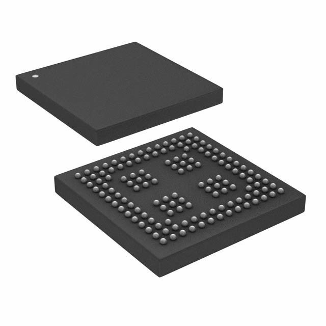
- Part No.:
- ADSP-21262SBBC-150
- Manufacturer:
- Analog Devices Inc.
- Category:
- DSP (Digital Signal Processors)
- Package:
- 136-LFBGA, CSPBGA
- Datasheet:
-
 ADSP-21262SBBC-150.pdf
- Description:
- IC DSP 32BIT 150MHZ 136CSBGA
- Quantity:
- Payment:

- Shipping:

Inventory:1,190
Please send an inquiry. Send us your inquiry, and we will respond immediately.
Product details
Overview
ADSP-21262SBBC-150 from Analog Devices is a 32-bit/40-bit floating-point SHARC DSP optimized for multichannel audio decoding and real-time signal processing in consumer AV receivers and home theater systems. It operates at 150 MHz (6.6 ns instruction cycle), integrates 2 Mbit dual-ported SRAM and 4 Mbit mask-programmable ROM, and supports Dolby Digital, DTS, and WMA-PRO 7.1 decoders preloaded in ROM.
For engineers reviewing the ADSP-21262SBBC-150 datasheet, ADSP-21262SBBC-150 pinout, ADSP-21262SBBC-150 application, or ADSP-21262SBBC-150 equivalent, key selection criteria include SIMD computational throughput (900 MFLOPS), ROM-based audio decoder availability, dual-ported memory bandwidth, DAI flexibility with PCGs and SRU routing, and BGA package compatibility for high-density audio subsystems.
Technical Context
The ADSP-21262SBBC-150 implements a dual-processing-element SIMD architecture (PEX and PEY), each with independent ALU, multiplier, shifter, and 32-register file, enabling parallel execution of identical instructions on distinct data streams. Its enhanced Harvard architecture sustains simultaneous 4×32-bit data transfers per core cycle via separate PM and DM buses.
It features a programmable digital application interface (DAI) with two precision clock generators (PCGs), an input data port (IDP) configurable as 8×I²S or 7-channel + 20-bit parallel acquisition, and a software-controlled signal routing unit (SRU) for dynamic peripheral interconnection. The on-chip PLL supports flexible core clock generation from external CLKIN using software-configurable numerator (1–64) and divisor (2, 4, 8, 16) values.
Key Specifications
| Parameter | Value and Actual Design Meaning |
|---|---|
| Core Instruction Rate | 150 MHz - delivers 900 MFLOPS SIMD performance; enables real-time execution of 96 kHz PCM, Dolby Pro Logic IIx, and DTS Neo:6 algorithms |
| On-Chip Memory | 2 Mbit dual-ported SRAM + 4 Mbit mask-ROM - supports concurrent core and I/O processor access; ROM contains certified multichannel decoders (Dolby Digital, DTS 96/24, WMA-PRO 7.1) |
| Digital Application Interface | 2 PCGs + IDP + SRU + 6 flag I/O + 3 timers - allows software-defined clock domain bridging, flexible audio data routing, and synchronized multichannel acquisition without external logic |
| Serial Ports | 6 full-duplex SPORTs - support up to 24 audio channels (I²S/left-justified) at ≤37.5 Mbps each; enable direct connection to AD183x codecs and multi-DAC systems |
| Power Supply Requirements | VDDINT = 1.2 V, VDDEXT = 3.3 V, AVDD = 1.2 V - AVDD powers internal PLL; requires dedicated analog filter (1nF/10nF/100nF + ferrite bead) for low-jitter clock generation |
| Package | 136-ball BGA (12 mm × 12 mm, 0.8 mm pitch) - matches footprint of ADSP-21266; supports high-speed signal integrity and thermal dissipation in compact AV receiver PCB layouts |
Pinout & Package
ADSP-21262SBBC-150 is housed in a 136-ball plastic ball grid array (PBGA) package with 0.8 mm pitch and 12 mm × 12 mm body size. Pin assignments follow the standardized 136-ball BGA configuration documented in Analog Devices' ADSP-2126x Rev. G datasheet (Pages 40–42), supporting JTAG emulation, parallel memory expansion, and high-bandwidth audio I/O.
| Pin/Terminal | Circuit Role | Design Meaning |
|---|---|---|
| CLKIN | External Clock Input | Accepts 12.288–50 MHz crystal or oscillator reference; feeds on-chip PLL to generate 150 MHz core clock |
| AVDD / AVSS | Analog Power / Ground | Powers internal PLL and precision clock generators; requires local RC-ferrite filter to maintain <100 fs RMS jitter for audio-grade timing |
| DAI_P0–P20 | Digital Application Interface Pins | Configurable as I²S data/clock/frame, PCG outputs, IDP inputs, or SRU-routed signals; enable hardware-agnostic peripheral integration |
| SPORT0–5 | Synchronous Serial Port I/O | Each provides Tx/Rx pair with independent DMA; supports TDM, I²S, and left-justified modes up to 32-bit word length |
| BMS0–BMS3 | Boot Mode Select | Configure boot source (SPI master/slave, parallel EPROM, internal ROM); determines initial code execution path at power-up |
Key Features
| Feature | Design Value |
|---|---|
| ROM-Based Audio Decoder Suite | Preprogrammed DTS Neo:6, Dolby Pro Logic IIx, WMA-PRO 7.1, and MPEG2 AAC LC decoders eliminate external firmware storage and reduce BOM cost in licensed AV receivers |
| Signal Routing Unit (SRU) | Software-configurable matrix interconnect for DAI peripherals-enables runtime reassignment of PCG clocks, IDP channels, and flag I/O without hardware changes |
| Dual-Ported Memory Architecture | 2 Mbit SRAM and 4 Mbit ROM accessible simultaneously by core and I/O processor-supports zero-wait-state audio buffering and background DMA transfers during real-time processing |
| 16-Bit Floating-Point Format Support | Single-instruction conversion between 32-bit and 16-bit FP formats doubles effective on-chip data storage density for coefficient tables and filter states |
| Hardware Circular Buffer Management | DAG1/DAG2 support 32 independent circular buffers with automatic wraparound-reduces overhead in FIR/IIR filters and FFT delay lines by eliminating manual pointer updates |
Applications
| Home Theater AV Receiver | Professional Audio Mixer |
|---|---|
Use Scenario: Real-time decoding and post-processing of 7.1-channel Dolby TrueHD and DTS-HD Master Audio bitstreams in premium AV receivers. IC Role / Device Role / Timing Role: Primary audio DSP executing ROM-resident decoders, applying room correction filters, and managing HDMI/SPDIF output timing via DAI PCGs. Use Value: Eliminates need for external decoder ASICs and reduces latency to <5 ms through on-chip SIMD acceleration and dual-ported memory concurrency. | Use Scenario: Low-latency mixing, dynamics processing, and effects rendering for 32-channel live sound consoles with analog I/O expansion. IC Role / Device Role / Timing Role: Central signal processor handling 6× full-duplex serial ports for ADC/DAC interfacing, 20-bit parallel acquisition for control surface data, and SRU-routed clock synchronization across multiple I/O cards. Use Value: Achieves sub-sample jitter (<2 ns) on all audio paths via AVDD-filtered PLL and PCG-derived sample clocks, meeting AES67 synchronization requirements. |
| Automotive Infotainment Head Unit | Digital Soundbar Processor |
Use Scenario: Multisource audio switching (Bluetooth A2DP, USB, FM tuner) with simultaneous Dolby Atmos and DTS:X decoding in automotive cockpit systems. IC Role / Device Role / Timing Role: Audio subsystem controller managing codec interfaces, ROM-based decoder execution, and CAN bus–triggered audio scene switching via GPIO flags. Use Value: Enables seamless source transitions with <100 ms mute time using ROM-resident decoder state machines and DMA-prefetched audio buffers. | Use Scenario: Compact soundbar implementing virtual surround, bass enhancement, and dialogue clarity algorithms for TV audio enhancement. IC Role / Device Role / Timing Role: Dedicated audio co-processor running fixed-point and floating-point algorithms on dual PEX/PEY units, fed by I²S from TV SoC and driving Class-D amplifier drivers. Use Value: Delivers 900 MFLOPS compute headroom for real-time 3D audio rendering while maintaining <1.5 W typical power draw via 1.2 V core supply optimization. |
Equivalent & Alternatives
The following parts are listed as comparable options for similar audio DSP applications.
| Alternative Part | Technical Difference | Application Difference | Selection Advice |
|---|---|---|---|
| ADSP-21262SBBCZ-150 | Same silicon, RoHS-compliant lead-free packaging (Pb-free solder compatible); identical electrical specs and ROM content | No functional difference; selected when lead-free manufacturing compliance is required | Direct drop-in replacement for ADSP-21262SBBC-150 in new designs targeting IPC-J-STD-020D reflow profiles |
| ADSP-21266SBBC-200 | Higher 200 MHz core (1200 MFLOPS), 4 Mbit ROM with expanded decoder set (includes WMA-PRO 7.1), same 136-ball BGA package | Enables higher channel count (9.1) and newer codecs (AAC-LC, MPEG2 BC) but consumes ~25% more power | Preferred when system-level performance margin is needed for future firmware upgrades or additional post-processing stages |
Compared with ADSP-21262SBBC-150, ADSP-21262SBBCZ-150 offers identical functionality in environmentally compliant packaging, while ADSP-21266SBBC-200 trades higher power for increased compute throughput and broader codec coverage-making the -150 optimal for cost-sensitive, thermally constrained AV receiver platforms where 900 MFLOPS suffices.
Availability
ADSP-21262SBBC-150 is available at Aetrix Electronics and suitable for home theater AV receivers, professional audio mixers, automotive infotainment head units, and digital soundbar processors requiring stable component supply and long-term lifecycle support.
Supply support for ADSP-21262SBBC-150 includes scheduled delivery planning, volume procurement assistance, BOM continuity management, traceable sourcing, and lifecycle availability coordination for OEM customers, industrial embedded developers, connected-device designers, and electronics production programs.
Manufacturer
Analog Devices, Inc. is a global semiconductor leader specializing in high-performance analog, mixed-signal, and digital signal processing technologies for precision instrumentation, industrial automation, and audio/video systems.
The ADSP-2126x SHARC family was designed specifically for high-fidelity, multichannel audio processing in licensed consumer electronics-integrating certified decoders, low-jitter clocking, and SIMD compute to replace discrete DSP + ASIC solutions in AV receivers and soundbars.
FAQ
What audio decoder algorithms are factory-programmed into the ROM of the ADSP-21262SBBC-150?
The ADSP-21262SBBC-150 includes factory-masked ROM containing Dolby Digital, DTS 96/24 5.1, DTS Neo:6, Dolby Pro Logic II, Dolby Pro Logic IIx, PCM 96 kHz, and MPEG2 BC 2ch decoders. Unlike the ADSP-21266 variant, it does not include WMA-PRO 7.1 or AAC-LC in ROM. These decoders execute directly from ROM without external firmware loading, reducing boot time and BOM cost in licensed AV receiver designs.
Does the ADSP-21262SBBC-150 support JTAG emulation and real-time debugging?
Yes, the ADSP-21262SBBC-150 implements IEEE 1149.1 JTAG test access port for full-speed emulation using Analog Devices CrossCore Embedded Studio or legacy VisualDSP++. It supports real-time memory/register inspection, breakpoint insertion, and stack tracing without affecting target system timing-critical for validating multichannel audio pipeline latency and interrupt response in production firmware development.
What is the maximum data rate supported by the serial ports on the ADSP-21262SBBC-150?
The six full-duplex serial ports (SPORTs) on the ADSP-21262SBBC-150 operate at up to one-quarter of the core clock rate. At 150 MHz, this yields a maximum data rate of 37.5 Mbps per SPORT. Each SPORT supports I²S, left-justified, TDM, and standard DSP serial modes with 3–32 bit word lengths, enabling direct interface to AD183x codecs and multi-channel DACs without external level-shifting or framing logic.
How does the Signal Routing Unit (SRU) enhance system design flexibility for the ADSP-21262SBBC-150?
The SRU in the ADSP-21262SBBC-150 is a software-configurable matrix that dynamically routes signals between DAI peripherals-including PCG outputs, IDP inputs, flag I/O, and timers. This eliminates fixed hardware interconnects, allowing runtime reassignment of clock domains, data paths, and control signals. For example, a single PCG output can be routed to multiple SPORT frame sync inputs, enabling synchronized multichannel acquisition across disparate audio subsystems without PCB redesign.
What power supply filtering is required for the AVDD pin on the ADSP-21262SBBC-150 to ensure low-jitter clock operation?
The AVDD pin on the ADSP-21262SBBC-150 must be filtered with a three-capacitor network (1 nF, 10 nF, 100 nF) and a ferrite bead (e.g., Murata BLM18AG102SN1D) placed within 2 mm of the AVDD/AVSS pins. This filter suppresses high-frequency noise coupling into the on-chip PLL, maintaining <100 fs RMS jitter-essential for maintaining THD+N < −105 dB in high-resolution audio playback applications using the ADSP-21262SBBC-150.
ADSP-21262SBBC-150 Specifications
- Product attributes
- Attribute value
- Manufacturer:
- Analog Devices Inc.
- Series:
- SHARC®
- Package/Case:
- 136-LFBGA, CSPBGA
- Packaging:
- Tray
- Product Status:
- Obsolete
- Type:
- Floating Point
- Interface:
- DAI, SPI
- Clock Rate:
- 150MHz
- Non-Volatile Memory:
- ROM (512kB)
- On-Chip RAM:
- 256kB
- Voltage - I/O:
- 3.30V
- Voltage - Core:
- 1.20V
- Operating Temperature:
- -40°C ~ 85°C (TA)
- Grade:
- -
- Qualification:
- -
- Mounting Type:
- Surface Mount
- Supplier Device Package:
- 136-CSPBGA (12x12)
ADSP-21262SBBC-150 FAQ
1.How can I place an order for ADSP-21262SBBC-150 through Aetrix?
Please submit a Request for Quotation (RFQ) for ADSP-21262SBBC-150 on Aetrix. Our sales agent will provide a competitive quotation and guide you through the order confirmation once you accept the terms.
2.Are the price and stock information for ADSP-21262SBBC-150 reliable?
The price and inventory of ADSP-21262SBBC-150 are updated periodically and may fluctuate due to market conditions. Stock and pricing data are typically refreshed every 24 hours. Quotation validity for ADSP-21262SBBC-150 is usually 5 days.
3.What payment methods are accepted for ADSP-21262SBBC-150?
We accept Wire Transfer, PayPal, Credit Card, Western Union, MoneyGram, and Escrow for ADSP-21262SBBC-150 transactions.
Note: Certain payment methods may incur a processing fee.
4.How is shipping managed for ADSP-21262SBBC-150?
ADSP-21262SBBC-150 orders can be shipped via leading logistics carriers, including DHL, UPS, FedEx, TNT, or Registered Mail.
Once your ADSP-21262SBBC-150 order is processed, you will receive an email with the shipment details and tracking number.
Note: Tracking information may take up to 24 hours to appear. Express delivery typically takes 3–5 business days.
5.How can I obtain technical support or documentation for ADSP-21262SBBC-150?
For technical support, including ADSP-21262SBBC-150 datasheets, pinout diagrams, or application guidance, please contact our engineering support team. They can provide detailed documentation and assistance for your ADSP-21262SBBC-150 requirements.
6.How does Aetrix verify that ADSP-21262SBBC-150 is sourced from the original manufacturer or authorized distributors?
All ADSP-21262SBBC-150 products on Aetrix are procured from qualified distributors and authorized channels. Our dedicated quality assurance team conducts strict verification, including traceability checks and, if necessary, third-party testing. This ensures that ADSP-21262SBBC-150 meets industry standards.
7.What is the process for return or replacement of ADSP-21262SBBC-150?
All ADSP-21262SBBC-150 units undergo pre-shipment inspection (PSI). If there is an issue with ADSP-21262SBBC-150, returns or replacements are accepted under the following conditions:
1.Quantity discrepancies, incorrect items, or visible external defects (such as breakage or corrosion), acknowledged by Aetrix.
2.The issue is reported within 90 days of delivery.
3.The ADSP-21262SBBC-150 part is unused and in its original packaging.
Return procedure for ADSP-21262SBBC-150:
1.Submit a request within 90 days.
2.Obtain a Return Material Authorization (RMA) from Aetrix.
ADSP-21262SBBC-150 Tags
-
TMS320C5535AZAY10
Texas Instruments
-
TMS320VC5501PGF300
Texas Instruments
-
ADSP-BF592KCPZ
Analog Devices Inc.
-
ADAU1463WBCPZ150
Analog Devices Inc.

-
TMS320VC5402PGE100
Texas Instruments

-
ADAU1701JSTZ-RL
Analog Devices Inc.
-
ADAU1701JSTZ
Analog Devices Inc.
-
TMS320VC5502PGF300
Texas Instruments
-
ADAU1462WBCPZ300RL
Analog Devices Inc.
-
ADAU1452KCPZRL
Analog Devices Inc.
-
ADAU1452WBCPZ-RL
Analog Devices Inc.
-
TMS320C6747DZKB3
Texas Instruments
Tech Hub

A practical engineering guide to 3.3V and 5V logic compatibility, input thresholds, resistor dividers, translator ICs, MOSFET level shifting, I2C pull-ups, timing limits and power-sequencing risks.

The 74HC595 uses push-pull logic outputs, while the TPIC6B595 uses 50 V open-drain DMOS sinks for higher-power loads. This guide compares timing, current limits, 3.3 V interfacing, load wiring, thermal…

The 74HC595 converts serial data into eight stable parallel outputs. This guide covers pin functions, shift and storage timing, OE and MR behavior, drive-current limits, cascading, voltage compatibilit…

A technical comparison of level-sensitive latches and edge-triggered flip-flops, covering timing windows, setup and hold limits, master–slave operation, time borrowing, race-through, HDL inference and…

A D latch stores one bit while Enable controls when data can pass. This reference covers gate-level operation, truth tables, transparency, setup and hold timing, LE versus OE, common ICs and practical …

An SR latch stores one bit through cross-coupled feedback. This engineering reference covers NOR and NAND implementations, truth tables, forbidden-state recovery, gated operation, switch debouncing, fa…

Latch circuits retain one bit through feedback. This technical reference covers SR and D latches, truth tables, transparency, timing limits, latch-versus-flip-flop behavior, applications and common log…

An engineering guide to LED driver operation, constant-current and constant-voltage outputs, linear and switching topologies, dimming, IC selection, calculations, replacement compatibility, and fault c…

Operational amplifier guide covering op amp basics, feedback, ideal vs real op amps, common configurations, buffer circuits, offset, bias current, gain-bandwidth, slew rate, rail-to-rail limits and sel…

Jumper cables guide covering safe connection order, red and black clamp placement, final ground connection, cable gauge, length, clamp quality, copper vs CCA cables, jump starter comparison and battery…


