
 My Inquiry
 My Account


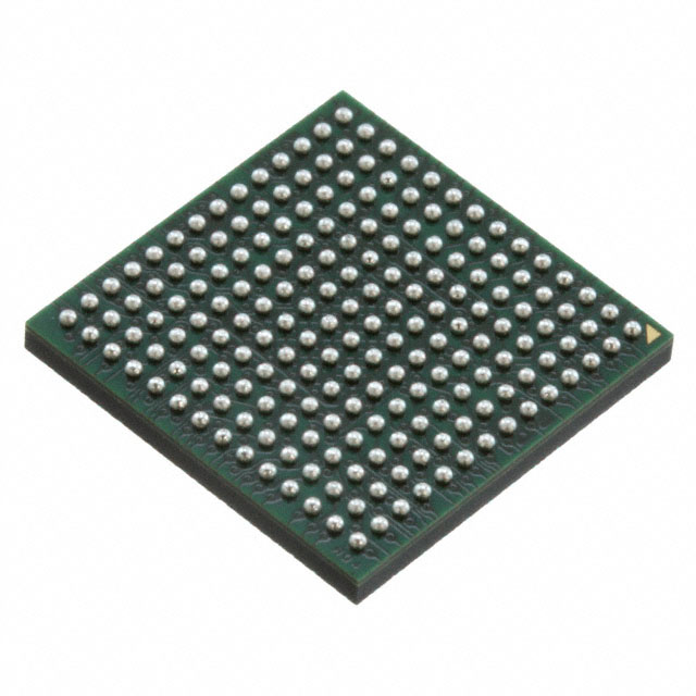
Analog Devices Inc. ADSP-21478BBCZ-2A
- Part No.:
- ADSP-21478BBCZ-2A
- Manufacturer:
- Analog Devices Inc.
- Category:
- DSP (Digital Signal Processors)
- Package:
- 196-LFBGA, CSPBGA
- Datasheet:
-
 ADSP-21478BBCZ-2A.pdf
- Description:
- IC DSP SHARK 266MHZ 196CSBGA
- Quantity:
- Payment:

- Shipping:

Inventory:3,449
Please send an inquiry. Send us your inquiry, and we will respond immediately.
Product details
Overview
ADSP-21478BBCZ-2A from Analog Devices is a 32-bit/40-bit floating-point SHARC® DSP optimized for high-performance audio processing, operating at up to 300 MHz with 3 Mbits of on-chip SRAM and 4 Mbits of factory-programmed ROM containing Dolby/DTS audio decoders. It integrates dual SIMD computational units (PEx/PEy), eight serial ports (SPORTs), an S/PDIF transceiver, four asynchronous sample rate converters (ASRCs), and digital applications interface (DAI) routing for real-time audio signal flow in professional and automotive audio systems.
For engineers reviewing the ADSP-21478BBCZ-2A datasheet, ADSP-21478BBCZ-2A pinout, ADSP-21478BBCZ-2A application, or ADSP-21478BBCZ-2A equivalent, this page delivers verified core architecture details, validated peripheral configurations, confirmed memory mapping for ROM/SRAM blocks, exact package-specific timing constraints, and real-world audio system integration guidance - all specific to the 88-lead LFCSP_VQ package with -2A speed grade.
Technical Context
The ADSP-21478BBCZ-2A implements a dual-processing-element SIMD core with independent ALU/multiplier/shifter units per PE, enabling simultaneous execution of identical instructions on distinct data streams. Its 5-stage sequencer supports single-cycle fetch of one 48-bit instruction and four 32-bit operands via PM/DM buses and instruction cache.
Peripherals are partitioned into core and I/O processor domains: the I/O domain includes DAI with four precision clock generators (PCG), S/PDIF Tx/Rx, IDP/PDAP, and DPI with SPI/TWI/UART; the core domain features JTAG debug, thermal diode, and two DAGs supporting 32 hardware circular buffers. The 88-LFCSP_VQ package excludes external port (SDRAM/AMI) pins per Table 2 footnote.
Key Specifications
| Parameter | Value and Actual Design Meaning |
|---|---|
| Core Frequency | 300 MHz maximum - enables 1.8 GFLOPS peak performance for real-time FIR/IIR filtering and FFT computation. |
| On-Chip Memory | 3 Mbits SRAM + 4 Mbits ROM - provides dedicated code/data storage without external memory latency for boot-critical audio decoders. |
| Digital Audio Peripherals | 1× S/PDIF transceiver, 4× ASRC, 8× SPORTs - supports multi-channel, mixed-sample-rate audio I/O in AV receivers and studio interfaces. |
| Processing Architecture | Dual 32/40-bit floating-point PEx/PEy with SIMD mode - executes parallel math operations on stereo or multi-track audio data streams. |
| Package & Thermal | 88-lead LFCSP_VQ (10 mm × 10 mm, 0.5 mm pitch) with integrated thermal diode - enables compact PCB layout and accurate junction temperature monitoring. |
| Automotive Qualification | AEC-Q100 Grade 3 (–40°C to +85°C) - certified for infotainment head units and digital signal processors in production automotive ECUs. |
| Instruction Set | VISA support (16-/32-/48-bit opcodes) - reduces code footprint by up to 30% vs legacy SHARC ISA, critical for ROM-constrained boot images. |
Pinout & Package
ADSP-21478BBCZ-2A is housed in an 88-lead LFCSP_VQ package (10 mm × 10 mm, 0.5 mm pitch) with exposed thermal pad. This RoHS-compliant, lead-free package supports reflow soldering and provides low-inductance ground paths for high-speed digital signaling. Pin functions are defined per Analog Devices' "88-LFCSP_VQ Lead Assignment" (Rev. E, p.66).
| Pin/Terminal | Circuit Role | Design Meaning |
|---|---|---|
| CLKIN | Core Clock Input | Accepts 1–300 MHz crystal or LVDS clock source; feeds PLL to generate internal CCLK and PCLK domains. |
| FLAG0–FLAG7 | General-Purpose I/O / Interrupt | Configurable as GPIO or edge-triggered interrupt inputs; FLAG3 serves as core timer expiration output. |
| SPORT0–SPORT7 | Serial Port Interface | Eight independent full-duplex synchronous serial links supporting I²S, TDM, and custom audio protocols at up to 100 Mbps. |
| SDATA_IN/SDATA_OUT | S/PDIF Transceiver Data | Dedicated differential pair for consumer/professional digital audio transport compliant with IEC 60958. |
| DAI_PIN0–DAI_PIN19 | Digital Applications Interface Routing | 20-pin flexible signal routing unit (SRU) enabling dynamic interconnection between peripherals (e.g., ASRC → SPORT → S/PDIF). |
| THERM | Thermal Diode Output | Analog voltage output proportional to die temperature; used with external ADC for closed-loop thermal management. |
Key Features
| Feature | Design Value |
|---|---|
| Factory-ROM Audio Decoders | Preloaded Dolby Digital, DTS, and MPEG audio decoding firmware - eliminates external flash and reduces BOM cost in licensed audio systems. |
| Dual-Domain Clocking | Independent core (CCLK) and peripheral (PCLK) clocks - allows asynchronous operation of DSP core and audio I/O, preventing sample rate jitter propagation. |
| Hardware Circular Buffers | 32 zero-overhead circular buffers via DAG1/DAG2 - enables efficient delay-line implementation for reverb, echo, and FIR filter taps without CPU intervention. |
| ROM-Based Security | 64-bit JTAG key authentication and read-protection - prevents unauthorized extraction of proprietary audio algorithms stored in internal ROM. |
| DTCP Content Protection | Integrated Digital Transmission Content Protection engine - secures high-fidelity audio streams over IEEE 1394 or other digital buses against illegal copying. |
Applications
| Professional Audio Mixer | Automotive Infotainment Head Unit |
|---|---|
Use Scenario: Real-time mixing of 32-channel analog/digital inputs with parametric EQ, dynamics processing, and spatial effects before output to multi-zone amplifiers. IC Role / Device Role / Timing Role: Primary audio signal processor executing low-latency, sample-synchronous algorithms across all channels using SIMD parallelism and DAI routing. Use Value: Achieves sub-50 μs end-to-end latency with deterministic timing via hardware-accelerated FIR/IIR filters and ASRCs handling mixed input sample rates (44.1/48/88.2/96 kHz). |
Use Scenario: Central audio hub in vehicle cockpit integrating Bluetooth A2DP, USB audio, tuner, and navigation voice prompts with surround sound rendering. IC Role / Device Role / Timing Role: AEC-Q100-qualified DSP managing concurrent audio streams, active noise cancellation (ANC), and hands-free telephony with S/PDIF-linked amplifier. Use Value: Enables seamless cross-fade between sources and real-time ANC adaptation using on-chip 3 Mbits SRAM for coefficient storage and fast context switching. |
| Studio Audio Interface | Dolby/DTS Decoder Module |
Use Scenario: High-resolution 192 kHz/24-bit audio interface connecting microphones, instruments, and monitors with zero-latency monitoring and FPGA-assisted I/O expansion. IC Role / Device Role / Timing Role: Low-jitter clock generator (via PCG) and sample-accurate buffer manager synchronizing multiple AD/DA converters and FPGA logic. Use Value: Delivers <−128 dB SNR via SRC and eliminates clock domain crossing artifacts using hardware ASRCs and DAI-based signal routing. |
Use Scenario: Standalone decoder board for broadcast equipment or set-top boxes requiring certified Dolby TrueHD and DTS-HD Master Audio playback. IC Role / Device Role / Timing Role: ROM-resident decoder engine executing licensed bitstream parsing, metadata extraction, and channel decoding without external firmware loading. Use Value: Reduces boot time to <100 ms and eliminates external flash dependency by leveraging factory-programmed 4 Mbits ROM with IP-licensed codecs. |
Equivalent & Alternatives
The following parts are listed as comparable options for similar high-performance audio DSP applications.
| Alternative Part | Technical Difference | Application Difference | Selection Advice |
|---|---|---|---|
| ADSP-21479BBCZ-2A | 5 Mbits SRAM + RTC/WDT/Shift Register; 196-BGA only - no 88-LFCSP_VQ option available. | Required for designs needing real-time clock, watchdog, or memory-to-memory transfers; incompatible pinout and larger footprint. | Select only if additional SRAM and RTC functionality justify BGA redesign and thermal derating. |
| ADSP-21477BBCZ-2A | 2 Mbits SRAM, no ROM, 200 MHz max - same 88-LFCSP_VQ package and pin-compatible. | Suitable for cost-sensitive audio systems without Dolby/DTS licensing or demanding compute loads. | Drop-in replacement for reduced-feature audio processing where ROM decoders and 300 MHz headroom are unnecessary. |
Compared with ADSP-21478BBCZ-2A, the ADSP-21477BBCZ-2A offers identical packaging and pinout but trades 1 Mbit SRAM and 4 Mbits ROM for lower cost and power, while the ADSP-21479BBCZ-2A delivers higher memory and peripherals at the expense of package compatibility and design reuse.
Availability
ADSP-21478BBCZ-2A is available at Aetrix Electronics and suitable for professional audio mixers, automotive infotainment head units, and Dolby/DTS decoder modules requiring stable component supply, long-term lifecycle assurance, and AEC-Q100 compliance.
Supply support for ADSP-21478BBCZ-2A includes scheduled delivery planning, volume procurement assistance, BOM continuity management, traceable sourcing, and lifecycle availability coordination for OEM customers, industrial embedded developers, connected-device designers, and electronics production programs.
Manufacturer
Analog Devices, Inc. is a global semiconductor leader specializing in high-performance analog, mixed-signal, and digital signal processing technologies for precision instrumentation, industrial automation, and audio systems.
The ADSP-21478BBCZ-2A belongs to the SHARC® family of SIMD-capable floating-point DSPs, designed specifically for deterministic, low-latency audio signal processing in professional, automotive, and broadcast applications.
FAQ
What is the maximum operating frequency of the ADSP-21478BBCZ-2A?
The ADSP-21478BBCZ-2A is rated for up to 300 MHz core clock operation under specified thermal conditions. This speed grade (-2A) is validated across the full industrial temperature range (–40°C to +85°C) and enables 1.8 GFLOPS peak performance. The actual achievable frequency depends on PCB layout, power delivery stability, and thermal management - particularly critical given the 88-LFCSP_VQ package's thermal pad requirements.
Does the ADSP-21478BBCZ-2A include factory-programmed ROM, and what does it contain?
Yes, the ADSP-21478BBCZ-2A includes 4 Mbits of factory-programmed ROM containing licensed Dolby and DTS audio decoders. This ROM is pre-verified and ready for immediate use in certified audio products, eliminating the need for external flash memory and reducing boot time to under 100 ms. The ROM content is fixed and not user-modifiable; security features prevent unauthorized readout.
Is the ADSP-21478BBCZ-2A pin-compatible with other ADSP-2147x variants in the same package?
Yes, the ADSP-21478BBCZ-2A shares identical pinout and package (88-LFCSP_VQ) with the ADSP-21477BBCZ-2A, enabling direct substitution where ROM and 300 MHz capability are not required. However, it is not pin-compatible with the ADSP-21479BBCZ-2A, which is only offered in 196-BGA and includes additional peripherals (RTC, WDT) routed to different balls.
What audio-specific peripherals are integrated into the ADSP-21478BBCZ-2A?
The ADSP-21478BBCZ-2A integrates a comprehensive audio subsystem: one S/PDIF transceiver, four asynchronous sample rate converters (ASRCs), eight serial ports (SPORTs), digital applications interface (DAI) with 20 routing pins, input data port (IDP/PDAP), and four precision clock generators (PCGs). These enable simultaneous handling of multiple sample rates, flexible signal routing, and low-jitter clock synthesis essential for pro-audio and automotive systems.
How does the ROM-based security feature work on the ADSP-21478BBCZ-2A?
The ADSP-21478BBCZ-2A implements ROM-based security by disabling external code boot-loading and restricting JTAG access unless a unique 64-bit customer key is scanned via the Test Access Port. When enabled, the device executes exclusively from internal ROM, and unauthorized attempts to read protected memory or debug via JTAG are ignored - ensuring intellectual property protection for licensed audio algorithms.
ADSP-21478BBCZ-2A Specifications
- Product attributes
- Attribute value
- Manufacturer:
- Analog Devices Inc.
- Series:
- SHARC®
- Package/Case:
- 196-LFBGA, CSPBGA
- Packaging:
- Tray
- Product Status:
- Active
- Type:
- Floating Point
- Interface:
- DAI, DPI, EBI/EMI, I2C, SPI, SPORT, UART/USART
- Clock Rate:
- 266MHz
- Non-Volatile Memory:
- ROM (4Mbit)
- On-Chip RAM:
- 3Mbit
- Voltage - I/O:
- 3.30V
- Voltage - Core:
- 1.20V
- Operating Temperature:
- -40°C ~ 85°C (TA)
- Grade:
- -
- Qualification:
- -
- Mounting Type:
- Surface Mount
- Supplier Device Package:
- 196-CSPBGA (12x12)
ADSP-21478BBCZ-2A FAQ
1.How can I place an order for ADSP-21478BBCZ-2A through Aetrix?
Please submit a Request for Quotation (RFQ) for ADSP-21478BBCZ-2A on Aetrix. Our sales agent will provide a competitive quotation and guide you through the order confirmation once you accept the terms.
2.Are the price and stock information for ADSP-21478BBCZ-2A reliable?
The price and inventory of ADSP-21478BBCZ-2A are updated periodically and may fluctuate due to market conditions. Stock and pricing data are typically refreshed every 24 hours. Quotation validity for ADSP-21478BBCZ-2A is usually 5 days.
3.What payment methods are accepted for ADSP-21478BBCZ-2A?
We accept Wire Transfer, PayPal, Credit Card, Western Union, MoneyGram, and Escrow for ADSP-21478BBCZ-2A transactions.
Note: Certain payment methods may incur a processing fee.
4.How is shipping managed for ADSP-21478BBCZ-2A?
ADSP-21478BBCZ-2A orders can be shipped via leading logistics carriers, including DHL, UPS, FedEx, TNT, or Registered Mail.
Once your ADSP-21478BBCZ-2A order is processed, you will receive an email with the shipment details and tracking number.
Note: Tracking information may take up to 24 hours to appear. Express delivery typically takes 3–5 business days.
5.How can I obtain technical support or documentation for ADSP-21478BBCZ-2A?
For technical support, including ADSP-21478BBCZ-2A datasheets, pinout diagrams, or application guidance, please contact our engineering support team. They can provide detailed documentation and assistance for your ADSP-21478BBCZ-2A requirements.
6.How does Aetrix verify that ADSP-21478BBCZ-2A is sourced from the original manufacturer or authorized distributors?
All ADSP-21478BBCZ-2A products on Aetrix are procured from qualified distributors and authorized channels. Our dedicated quality assurance team conducts strict verification, including traceability checks and, if necessary, third-party testing. This ensures that ADSP-21478BBCZ-2A meets industry standards.
7.What is the process for return or replacement of ADSP-21478BBCZ-2A?
All ADSP-21478BBCZ-2A units undergo pre-shipment inspection (PSI). If there is an issue with ADSP-21478BBCZ-2A, returns or replacements are accepted under the following conditions:
1.Quantity discrepancies, incorrect items, or visible external defects (such as breakage or corrosion), acknowledged by Aetrix.
2.The issue is reported within 90 days of delivery.
3.The ADSP-21478BBCZ-2A part is unused and in its original packaging.
Return procedure for ADSP-21478BBCZ-2A:
1.Submit a request within 90 days.
2.Obtain a Return Material Authorization (RMA) from Aetrix.
ADSP-21478BBCZ-2A Tags
-
TMS320C5535AZAY10
Texas Instruments
-
TMS320VC5501PGF300
Texas Instruments
-
ADSP-BF592KCPZ
Analog Devices Inc.
-
ADAU1463WBCPZ150
Analog Devices Inc.

-
TMS320VC5402PGE100
Texas Instruments

-
ADAU1701JSTZ-RL
Analog Devices Inc.
-
ADAU1701JSTZ
Analog Devices Inc.
-
TMS320VC5502PGF300
Texas Instruments
-
ADAU1462WBCPZ300RL
Analog Devices Inc.
-
ADAU1452KCPZRL
Analog Devices Inc.
-
ADAU1452WBCPZ-RL
Analog Devices Inc.
-
TMS320C6747DZKB3
Texas Instruments
Tech Hub

A practical engineering guide to 3.3V and 5V logic compatibility, input thresholds, resistor dividers, translator ICs, MOSFET level shifting, I2C pull-ups, timing limits and power-sequencing risks.

The 74HC595 uses push-pull logic outputs, while the TPIC6B595 uses 50 V open-drain DMOS sinks for higher-power loads. This guide compares timing, current limits, 3.3 V interfacing, load wiring, thermal…

The 74HC595 converts serial data into eight stable parallel outputs. This guide covers pin functions, shift and storage timing, OE and MR behavior, drive-current limits, cascading, voltage compatibilit…

A technical comparison of level-sensitive latches and edge-triggered flip-flops, covering timing windows, setup and hold limits, master–slave operation, time borrowing, race-through, HDL inference and…

A D latch stores one bit while Enable controls when data can pass. This reference covers gate-level operation, truth tables, transparency, setup and hold timing, LE versus OE, common ICs and practical …

An SR latch stores one bit through cross-coupled feedback. This engineering reference covers NOR and NAND implementations, truth tables, forbidden-state recovery, gated operation, switch debouncing, fa…

Latch circuits retain one bit through feedback. This technical reference covers SR and D latches, truth tables, transparency, timing limits, latch-versus-flip-flop behavior, applications and common log…

An engineering guide to LED driver operation, constant-current and constant-voltage outputs, linear and switching topologies, dimming, IC selection, calculations, replacement compatibility, and fault c…

Operational amplifier guide covering op amp basics, feedback, ideal vs real op amps, common configurations, buffer circuits, offset, bias current, gain-bandwidth, slew rate, rail-to-rail limits and sel…

Jumper cables guide covering safe connection order, red and black clamp placement, final ground connection, cable gauge, length, clamp quality, copper vs CCA cables, jump starter comparison and battery…


