
 My Inquiry
 My Account


Analog Devices Inc. ADSP-21488KSWZ-4B1
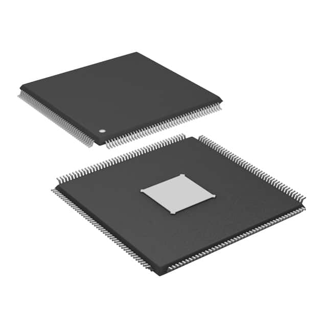
- Part No.:
- ADSP-21488KSWZ-4B1
- Manufacturer:
- Analog Devices Inc.
- Category:
- DSP (Digital Signal Processors)
- Package:
- 176-LQFP Exposed Pad
- Datasheet:
-
 ADSP-21488KSWZ-4B1.pdf
- Description:
- IC CCD SIGNAL PROCESSOR 176LQFP
- Quantity:
- Payment:

- Shipping:

Inventory:4,469
Please send an inquiry. Send us your inquiry, and we will respond immediately.
Product details
Overview
ADSP-21488KSWZ-4B1 from Analog Devices is a 32-bit/40-bit floating-point SHARC® DSP optimized for high-performance audio processing in automotive and professional audio systems. It operates at up to 400 MHz, integrates 3 Mbits of on-chip SRAM and 4 Mbits of mask-ROM, and features SIMD computational architecture with dual processing elements (PEx/PEy), enabling 2.16 GFLOPS peak performance. Its digital applications interface (DAI) includes S/PDIF transceiver, four asynchronous sample rate converters (ASRC), eight serial ports (SPORT), and precision clock generators - all supporting real-time multichannel audio routing and processing.
For engineers reviewing the ADSP-21488KSWZ-4B1 datasheet, ADSP-21488KSWZ-4B1 pinout, ADSP-21488KSWZ-4B1 application, or ADSP-21488KSWZ-4B1 equivalent, key selection criteria include its AEC-Q100 qualification, 88-lead LFCSP_VQ package, 400 MHz core frequency, ROM-based audio decoder support, and absence of external port (SDRAM/AMI) due to package constraints - critical for space-constrained automotive infotainment and premium audio head units.
Technical Context
The ADSP-21488KSWZ-4B1 implements a dual-processing-element SIMD core with independent ALU, multiplier, shifter, and 16-register data files per element (R0–R15/S0–S15), enabling parallel execution of identical instructions on distinct data streams. Its enhanced Harvard architecture supports simultaneous 48-bit instruction fetch from cache and four 32-bit operand transfers via PM/DM buses - sustaining full-speed FIR, IIR, and FFT operations without pipeline stalls.
Peripherally, it integrates a fully configurable DAI with SRU routing, S/PDIF Tx/Rx, four ASRCs (–128 dB THD+N), eight SPORTs, and IDP/PDAP for serial/parallel interconnect - all clocked by four independent PCGs. The absence of external port pins in the 88-lead LFCSP_VQ package eliminates SDRAM/AMI interface capability, distinguishing it from 100- and 176-lead variants.
Key Specifications
| Parameter | Value and Actual Design Meaning |
|---|---|
| Core Architecture | 32-bit/40-bit floating-point SIMD SHARC® with PEx/PEy dual processing elements and 5-stage sequencer |
| Max Core Frequency | 400 MHz - delivers 2.16 GFLOPS peak compute, validated for real-time 1024-point FFT in 23 μs |
| On-Chip Memory | 3 Mbits SRAM (configurable as 160k × 32-bit or mixed word sizes) + 4 Mbits mask-ROM with Dolby/DTS audio decoders |
| Package | 88-lead LFCSP_VQ (12 mm × 12 mm, 0.5 mm pitch) - no external port pins; SDRAM/AMI disabled |
| Automotive Qualification | AEC-Q100 Grade 2 (–40°C to +105°C ambient) - qualified for front/rear infotainment ECUs and amplifier modules |
| Digital Audio Peripherals | S/PDIF transceiver, 4× ASRC (–128 dB performance), 8× SPORT, IDP/PDAP, 4× PWM, TWI, SPI, UART, and DAI/DPI SRU routing |
| Security | ROM-based boot security with 64-bit JTAG key authentication - prevents unauthorized code readout and external boot loading |
Pinout & Package
ADSP-21488KSWZ-4B1 is housed in an 88-lead LFCSP_VQ (Lead Frame Chip Scale Package, Very Thin Quad Flat No-Lead) measuring 12 mm × 12 mm with 0.5 mm pitch and exposed thermal pad. This package omits all external port (EP) pins - disabling SDRAM and AMI interfaces - and reduces pin count versus 100- and 176-lead LQFP_EP variants. Thermal diode and power management pins are retained for automotive thermal monitoring.
| Pin/Terminal | Circuit Role | Design Meaning |
|---|---|---|
| VDD_IO / VDD_INT | Power supply rails | Separate 3.3 V I/O and 1.2 V core supplies - enables low-noise analog audio subsystem integration |
| CLKIN / CLKOUT | Master clock input/output | Accepts 1–50 MHz crystal or CMOS clock; CLKOUT drives external codecs or ASRC reference clocks |
| DAI_Px / DAI_Nx | Digital Applications Interface pins | Differential S/PDIF Tx/Rx, SPORT data/clock, PCG outputs - support multichannel TDM, I²S, and custom audio protocols |
| IDP0–IDP7 / PDAP0–PDAP7 | Input Data Port / Parallel Data Access Port | 8-bit parallel interface for ADC/DAC bridging or FPGA co-processing - configurable as input-only or bidirectional |
| FLAG0–FLAG3 | General-purpose I/O / interrupt flags | Programmable as GPIO, timer expiration signals, or external interrupt inputs - FLAG3 used for core timer expiry |
| TCK/TMS/TDO/TDI | JTAG test access port | IEEE 1149.1-compliant debug interface with 64-bit security key scan - required for secure emulation and firmware update |
Key Features
| Feature | Design Value |
|---|---|
| SIMD Computational Engine | Dual PEx/PEy elements execute identical instructions on separate data streams - doubles throughput for FIR/IIR filters and FFTs without software restructuring |
| Variable Instruction Set Architecture (VISA) | Supports 16-/32-/48-bit instructions - reduces code size by ~35% vs legacy ISA, lowering external memory bandwidth demand |
| Digital Applications Interface (DAI) | Hardware SRU routes signals between 8 SPORTs, S/PDIF, ASRCs, PCGs, and IDP/PDAP - eliminates FPGA glue logic for audio matrix switching |
| ROM-Based Audio Security & Decoding | Factory-programmed Dolby/DTS multichannel decoders + boot lock - ensures IP protection and eliminates external codec licensing in premium audio systems |
| AEC-Q100 Automotive Compliance | Qualified to Grade 2 (–40°C to +105°C) with integrated thermal diode - enables deployment in dashboard head units without external temperature sensors |
Applications
| Automotive Infotainment Head Unit | Premium Multi-Zone Audio Amplifier |
|---|---|
|
Use Scenario: Central audio processor in vehicle head unit managing Bluetooth streaming, USB playback, navigation voice prompts, and rear-seat entertainment. IC Role / Device Role / Timing Role: Real-time audio mixing, sample rate conversion (ASRC), Dolby Digital decoding (ROM-based), and S/PDIF output to amplifier. Use Value: Eliminates need for external audio codec and FPGA; 400 MHz core handles concurrent 8-channel decode + 32-band EQ + dynamic range control within 5 ms latency. |
Use Scenario: Channel-specific DSP in 16-channel Class-D amplifier for luxury vehicles, performing active crossover, time alignment, and speaker protection. IC Role / Device Role / Timing Role: Low-latency FIR filter engine for acoustic correction, with SPORTs feeding ADC data and driving PWM-modulated gate drivers. Use Value: On-chip 3 Mbits SRAM stores 16-channel FIR coefficients; SIMD execution achieves sub-100 μs filter latency per channel at 96 kHz sampling. |
| Professional Digital Mixer Console | High-End Home Theater AV Receiver |
|
Use Scenario: Embedded DSP engine in compact stage mixer handling mic preamp modeling, dynamics processing, and monitor mix routing. IC Role / Device Role / Timing Role: DAI SRU configures 8 SPORTs as I²S inputs/outputs; PCGs generate independent sample clocks for multi-rate sources. Use Value: Four ASRCs enable seamless integration of 44.1 kHz, 48 kHz, and 96 kHz sources without external resampling ICs - reducing BOM and jitter. |
Use Scenario: Core audio processor in 11.2-channel AV receiver performing object-based audio decoding (Dolby Atmos), room correction, and bass management. IC Role / Device Role / Timing Role: ROM-hosted Dolby Atmos decoder + real-time Dirac Live room correction using on-chip FFT/FIR accelerators. Use Value: Mask-ROM eliminates external flash storage and boot firmware validation; thermal diode enables fanless chassis design compliant with CE noise limits. |
Equivalent & Alternatives
The following parts are listed as comparable options for similar high-performance audio DSP applications.
| Alternative Part | Technical Difference | Application Difference | Selection Advice |
|---|---|---|---|
| ADSP-21489KSWZ-4A | 450 MHz core, 5 Mbits SRAM, 176-lead LQFP_EP package with full SDRAM/AMI interface | Supports external DDR2 memory expansion and complex system-level buffering - suitable for scalable multi-processor audio platforms | Select when >400 MHz compute, >3 Mbits RAM, or external memory interfacing is required; not pin-compatible with ADSP-21488KSWZ-4B1 |
| ADSP-21486KSWZ-4A | 400 MHz core, 5 Mbits SRAM, 100-lead LQFP_EP package - includes SDRAM controller but no AMI | Enables cost-optimized external memory use in mid-tier automotive audio without full 176-pin footprint | Choose for balanced memory capacity and external DRAM support in space-constrained designs where 88-pin LFCSP is insufficient |
Compared with ADSP-21488KSWZ-4B1, the ADSP-21489KSWZ-4A offers higher compute and memory but requires PCB redesign for 176-pin LQFP; the ADSP-21486KSWZ-4A provides more on-chip RAM than ADSP-21488KSWZ-4B1 while retaining 400 MHz operation and adding SDRAM support in a 100-pin package - making it a functional upgrade path without architectural change.
Availability
ADSP-21488KSWZ-4B1 is available at Aetrix Electronics and suitable for automotive infotainment, premium audio amplifiers, professional digital mixers, and high-end home theater receivers requiring stable component supply across extended product lifecycles.
Supply support for ADSP-21488KSWZ-4B1 includes scheduled delivery planning, volume procurement assistance, BOM continuity management, traceable sourcing, and lifecycle availability coordination for OEM customers, industrial embedded developers, connected-device designers, and electronics production programs.
Manufacturer
Analog Devices, Inc. is a global leader in high-performance analog, mixed-signal, and DSP technology, headquartered in Wilmington, MA, with deep expertise in signal processing for audio, industrial, and automotive markets.
The ADSP-21488KSWZ-4B1 belongs to the SHARC® family of SIMD floating-point DSPs, designed specifically for deterministic, low-latency audio processing in safety-critical and resource-constrained environments - emphasizing ROM security, AEC-Q100 compliance, and peripheral integration for end-to-end audio signal chains.
FAQ
What is the maximum operating frequency of the ADSP-21488KSWZ-4B1?
The ADSP-21488KSWZ-4B1 is rated for a maximum core clock frequency of 400 MHz, delivering 2.16 GFLOPS peak performance. This frequency is guaranteed across the full AEC-Q100 Grade 2 temperature range (–40°C to +105°C ambient) and is validated using the 1024-point complex FFT benchmark at 23 μs execution time. Operation above 400 MHz is not supported or characterized.
Does the ADSP-21488KSWZ-4B1 support external SDRAM or asynchronous memory interfaces?
No, the ADSP-21488KSWZ-4B1 in the 88-lead LFCSP_VQ package does not support external SDRAM or asynchronous memory interfaces. All external port (EP) pins - including SDRAM address/data/control and AMI signals - are omitted from this package variant. The Ordering Guide and Pin Function Descriptions explicitly state that SDRAM controller pins must be disabled when using the 88-lead package.
What audio decoders are included in the on-chip ROM of the ADSP-21488KSWZ-4B1?
The ADSP-21488KSWZ-4B1 includes factory-programmed multichannel audio decoding and post-processing algorithms from Dolby® Labs and DTS® in its 4 Mbits of mask-ROM. Specific decoder combinations (e.g., Dolby Digital Plus, DTS-HD Master Audio) depend on chip version and system configuration; full details are available in the latest Analog Devices audio decoder support documentation.
Is the ADSP-21488KSWZ-4B1 pin-compatible with other ADSP-2148x family members?
No, the ADSP-21488KSWZ-4B1 is not pin-compatible with other ADSP-2148x variants. It uses an 88-lead LFCSP_VQ package, whereas ADSP-21483/21486/21487/21489 are offered in 100- or 176-lead LQFP_EP packages. Pin functions, counts, and peripheral availability (e.g., missing EP pins) differ significantly - requiring unique PCB layout and schematic design.
How does the ROM-based security feature work on the ADSP-21488KSWZ-4B1?
The ADSP-21488KSWZ-4B1 implements ROM-based security by preventing boot-loading of external code and restricting JTAG access. A unique 64-bit key must be scanned via JTAG before emulation or debugging is enabled; incorrect keys are ignored. When activated, the processor executes exclusively from internal ROM, blocking unauthorized readout of protected firmware.
ADSP-21488KSWZ-4B1 Specifications
- Product attributes
- Attribute value
- Manufacturer:
- Analog Devices Inc.
- Series:
- SHARC®
- Package/Case:
- 176-LQFP Exposed Pad
- Packaging:
- Tray
- Product Status:
- Active
- Type:
- Floating Point
- Interface:
- EBI/EMI, DAI, I2C, SPI, SPORT, UART/USART
- Clock Rate:
- 400MHz
- Non-Volatile Memory:
- External
- On-Chip RAM:
- 3Mbit
- Voltage - I/O:
- 3.30V
- Voltage - Core:
- 1.10V
- Operating Temperature:
- 0°C ~ 70°C (TA)
- Grade:
- -
- Qualification:
- -
- Mounting Type:
- Surface Mount
- Supplier Device Package:
- 176-LQFP-EP (24x24)
ADSP-21488KSWZ-4B1 FAQ
1.How can I place an order for ADSP-21488KSWZ-4B1 through Aetrix?
Please submit a Request for Quotation (RFQ) for ADSP-21488KSWZ-4B1 on Aetrix. Our sales agent will provide a competitive quotation and guide you through the order confirmation once you accept the terms.
2.Are the price and stock information for ADSP-21488KSWZ-4B1 reliable?
The price and inventory of ADSP-21488KSWZ-4B1 are updated periodically and may fluctuate due to market conditions. Stock and pricing data are typically refreshed every 24 hours. Quotation validity for ADSP-21488KSWZ-4B1 is usually 5 days.
3.What payment methods are accepted for ADSP-21488KSWZ-4B1?
We accept Wire Transfer, PayPal, Credit Card, Western Union, MoneyGram, and Escrow for ADSP-21488KSWZ-4B1 transactions.
Note: Certain payment methods may incur a processing fee.
4.How is shipping managed for ADSP-21488KSWZ-4B1?
ADSP-21488KSWZ-4B1 orders can be shipped via leading logistics carriers, including DHL, UPS, FedEx, TNT, or Registered Mail.
Once your ADSP-21488KSWZ-4B1 order is processed, you will receive an email with the shipment details and tracking number.
Note: Tracking information may take up to 24 hours to appear. Express delivery typically takes 3–5 business days.
5.How can I obtain technical support or documentation for ADSP-21488KSWZ-4B1?
For technical support, including ADSP-21488KSWZ-4B1 datasheets, pinout diagrams, or application guidance, please contact our engineering support team. They can provide detailed documentation and assistance for your ADSP-21488KSWZ-4B1 requirements.
6.How does Aetrix verify that ADSP-21488KSWZ-4B1 is sourced from the original manufacturer or authorized distributors?
All ADSP-21488KSWZ-4B1 products on Aetrix are procured from qualified distributors and authorized channels. Our dedicated quality assurance team conducts strict verification, including traceability checks and, if necessary, third-party testing. This ensures that ADSP-21488KSWZ-4B1 meets industry standards.
7.What is the process for return or replacement of ADSP-21488KSWZ-4B1?
All ADSP-21488KSWZ-4B1 units undergo pre-shipment inspection (PSI). If there is an issue with ADSP-21488KSWZ-4B1, returns or replacements are accepted under the following conditions:
1.Quantity discrepancies, incorrect items, or visible external defects (such as breakage or corrosion), acknowledged by Aetrix.
2.The issue is reported within 90 days of delivery.
3.The ADSP-21488KSWZ-4B1 part is unused and in its original packaging.
Return procedure for ADSP-21488KSWZ-4B1:
1.Submit a request within 90 days.
2.Obtain a Return Material Authorization (RMA) from Aetrix.
ADSP-21488KSWZ-4B1 Tags
-
TMS320C5535AZAY10
Texas Instruments
-
TMS320VC5501PGF300
Texas Instruments
-
ADSP-BF592KCPZ
Analog Devices Inc.
-
ADAU1463WBCPZ150
Analog Devices Inc.

-
TMS320VC5402PGE100
Texas Instruments

-
ADAU1701JSTZ-RL
Analog Devices Inc.
-
ADAU1701JSTZ
Analog Devices Inc.
-
TMS320VC5502PGF300
Texas Instruments
-
ADAU1462WBCPZ300RL
Analog Devices Inc.
-
ADAU1452KCPZRL
Analog Devices Inc.
-
ADAU1452WBCPZ-RL
Analog Devices Inc.
-
TMS320C6747DZKB3
Texas Instruments
Tech Hub

A practical engineering guide to 3.3V and 5V logic compatibility, input thresholds, resistor dividers, translator ICs, MOSFET level shifting, I2C pull-ups, timing limits and power-sequencing risks.

The 74HC595 uses push-pull logic outputs, while the TPIC6B595 uses 50 V open-drain DMOS sinks for higher-power loads. This guide compares timing, current limits, 3.3 V interfacing, load wiring, thermal…

The 74HC595 converts serial data into eight stable parallel outputs. This guide covers pin functions, shift and storage timing, OE and MR behavior, drive-current limits, cascading, voltage compatibilit…

A technical comparison of level-sensitive latches and edge-triggered flip-flops, covering timing windows, setup and hold limits, master–slave operation, time borrowing, race-through, HDL inference and…

A D latch stores one bit while Enable controls when data can pass. This reference covers gate-level operation, truth tables, transparency, setup and hold timing, LE versus OE, common ICs and practical …

An SR latch stores one bit through cross-coupled feedback. This engineering reference covers NOR and NAND implementations, truth tables, forbidden-state recovery, gated operation, switch debouncing, fa…

Latch circuits retain one bit through feedback. This technical reference covers SR and D latches, truth tables, transparency, timing limits, latch-versus-flip-flop behavior, applications and common log…

An engineering guide to LED driver operation, constant-current and constant-voltage outputs, linear and switching topologies, dimming, IC selection, calculations, replacement compatibility, and fault c…

Operational amplifier guide covering op amp basics, feedback, ideal vs real op amps, common configurations, buffer circuits, offset, bias current, gain-bandwidth, slew rate, rail-to-rail limits and sel…

Jumper cables guide covering safe connection order, red and black clamp placement, final ground connection, cable gauge, length, clamp quality, copper vs CCA cables, jump starter comparison and battery…


