
 My Inquiry
 My Account


Analog Devices Inc. ADSP-2185LBCA-210
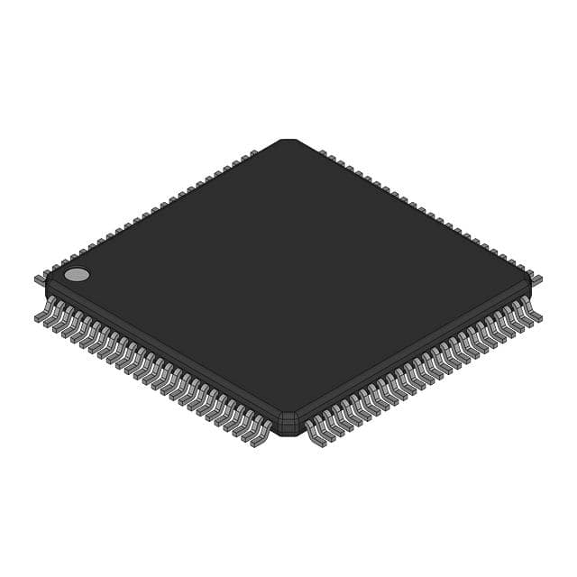
- Part No.:
- ADSP-2185LBCA-210
- Manufacturer:
- Analog Devices Inc.
- Category:
- DSP (Digital Signal Processors)
- Package:
- 144-LFBGA, CSPBGA
- Datasheet:
-
 ADSP-2185LBCA-210.pdf
- Description:
- IC DSP 16BIT 80MHZ 144CSPBGA
- Quantity:
- Payment:

- Shipping:

Inventory:7,235
Please send an inquiry. Send us your inquiry, and we will respond immediately.
Product details
Overview
ADSP-2185LBCA-210 from Analog Devices is a 33 MIPS fixed-point DSP microcomputer with 16K × 24-bit on-chip program RAM, 16K × 16-bit on-chip data RAM, and dual 16-bit synchronous serial ports (SPORT0/SPORT1). It executes instructions in 30 ns cycles, supports zero-overhead looping, and targets real-time audio processing, telecom channel coding, and embedded control systems requiring deterministic low-latency computation.
For engineers reviewing the ADSP-2185LBCA-210 datasheet, ADSP-2185LBCA-210 pinout, ADSP-2185LBCA-210 application, or ADSP-2185LBCA-210 equivalent, key selection criteria include instruction cycle time, on-chip memory configuration, serial port companding support (A-law/µ-law per G.711), power-down recovery latency (100 CLKIN cycles), and ICE-Port™ debug interface compatibility.
Technical Context
The ADSP-2185LBCA-210 implements the ADSP-2100 family base architecture with three independent computational units (ALU, MAC, shifter), two dedicated data address generators (DAGs), and a zero-overhead program sequencer. Its 3-bus architecture enables simultaneous dual operand fetches - one from program memory and one from data memory - in every instruction cycle.
It integrates a 16-bit internal DMA port (IDMA) for host-mode system interfacing, an 8-bit byte DMA port (BDMA) supporting up to 4 MByte external memory, and programmable 13-flag I/O with concurrent interrupt/flag functionality on multiplexed pins (e.g., IRQ2/PF7, IRQE/PF4).
Key Specifications
| Parameter | Value and Actual Design Meaning |
|---|---|
| Instruction Cycle Time | 30 ns - enables 33 MIPS sustained throughput for real-time signal processing loops. |
| On-Chip Program Memory | 16K × 24-bit RAM - stores both instructions and data; eliminates external program memory access latency. |
| On-Chip Data Memory | 16K × 16-bit RAM - supports dual-operand fetches and circular buffer addressing via DAGs. |
| Serial Ports | 2 × bidirectional SPORTs - each with hardware A-law/µ-law companding per CCITT G.711 and double-buffered transmit/receive. |
| Power-Down Recovery | 100 CLKIN cycles - allows rapid wake-up from ultra-low-power state without firmware reinitialization. |
| Package | 100-lead TQFP - surface-mount compatible with standard PCB assembly; pin-compatible with ADSP-2181/2186 in same footprint. |
| Clock Input | CLKIN at 16.67 MHz (half-instruction rate) - generates internal 33 MHz core clock; supports crystal or TTL clock source. |
Pinout & Package
ADSP-2185LBCA-210 is housed in a 100-lead Thin Quad Flat Package (TQFP) with 0.5 mm pitch, 14 mm × 14 mm body size, and exposed thermal pad. Pin functions are mode-dependent: Full Memory Mode uses A13–A0 and D23–D0 for external addressing/data; Host Mode repurposes pins as IAD15–IAD0, IWR, IRD, and IACK for IDMA interfacing.
| Pin/Terminal | Circuit Role | Design Meaning |
|---|---|---|
| RESET | Asynchronous processor reset input | Active-low signal that initializes registers, clears stacks, and forces boot sequence from external EPROM or internal DMA port. |
| CLKIN / XTAL | Clock source interface | Dual-function pins: accept 16.67 MHz TTL clock or connect parallel-resonant crystal (fundamental mode) for self-clocked operation. |
| SPORT0 / SPORT1 | Synchronous serial I/O interface | Each port provides 5 pins (SCLK, RFS, TFS, DT, DR); software-configurable for frame sync polarity, word length (3–16 bits), and companding. |
| PWD / PWDACK | Hardware power management control | PWD asserts low to enter power-down; PWDACK goes high when internal state is saved and clocks halted - confirms entry into 1 µA standby mode. |
| IRQ2/PF7, IRQE/PF4, etc. | Multiplexed interrupt/flag I/O | Shared pins retain both functions: e.g., IRQ2 triggers interrupt vector 0x0004; PF7 operates as general-purpose output flag when IMASK disables IRQ2. |
Key Features
| Feature | Design Value |
|---|---|
| Single-cycle instruction execution | Every ALU/MAC/shifter operation completes in one 30 ns cycle - enables deterministic timing for hard real-time control loops. |
| Zero-overhead looping | Hardware loop counters and stack eliminate branch penalties - critical for FFT, FIR, and correlation kernels with tight iteration counts. |
| ICE-Port™ emulator interface | 14-pin dedicated debug port supporting in-target operation, 20 breakpoints, and C-source-level debugging without target board modification. |
| Programmable memory strobes | Configurable wait-state generation per memory space (program/data/byte/I/O) - enables "glueless" interfacing with slow peripherals like EPROMs or LCD controllers. |
| UART emulation via SPORT | Software-reconfigurable SPORT pins emulate UART framing and baud rate generation - reduces BOM count in mixed-protocol embedded systems. |
Applications
| Voice Codec Implementation | Industrial Motor Control |
|---|---|
Use Scenario: Real-time voice encoding/decoding in VoIP gateways using G.711 A-law companding. IC Role / Device Role / Timing Role: Primary DSP executing adaptive differential pulse-code modulation (ADPCM) and echo cancellation algorithms with sub-100 µs latency. Use Value: On-chip SPORT hardware companding offloads 20% CPU cycles vs. software-only implementation; 16K data RAM holds dual-channel circular buffers for full-duplex operation. | Use Scenario: Closed-loop field-oriented control (FOC) of 3-phase BLDC motors in factory automation drives. IC Role / Device Role / Timing Role: Real-time PWM waveform synthesis and current-sensing ADC post-processing with deterministic 50 µs control loop timing. Use Value: Dual DAGs enable simultaneous sampling of three phase currents and updating of six PWM compare registers - eliminating external DMA arbitration delays. |
| Medical Ultrasound Beamforming | Secure Wireless Sensor Node |
Use Scenario: Digital beamforming in portable ultrasound systems using time-delay-and-sum algorithms across 64 channels. IC Role / Device Role / Timing Role: High-throughput data router and multiplier accumulator performing 128×128 complex multiply-accumulate operations per frame. Use Value: 40-bit MAC accumulator prevents overflow in multi-stage filtering; 80 KB on-chip RAM stores channel calibration coefficients and raw RF samples. | Use Scenario: Battery-powered environmental sensor node performing FFT-based spectral analysis on vibration data before encrypted transmission. IC Role / Device Role / Timing Role: Low-power analytics engine executing sleep-wake cycles triggered by accelerometer interrupts and waking only for scheduled FFT bursts. Use Value: Power-down mode draws <1 µA; 100-cycle wake-up ensures sensor fusion completes within 3 ms - meeting ISO 13849 response time requirements. |
Equivalent & Alternatives
The following parts are listed as comparable options for similar fixed-point DSP microcomputer applications.
| Alternative Part | Technical Difference | Application Difference | Selection Advice |
|---|---|---|---|
| ADSP-2186LBCA-210 | Same 100-lead TQFP package; adds 2K × 24-bit boot ROM and enhanced timer with capture/compare registers. | Better suited for systems requiring secure boot or precise PWM edge timing without external logic. | Select ADSP-2186LBCA-210 if boot ROM persistence or advanced timer features are required; otherwise ADSP-2185LBCA-210 offers lower cost and identical core performance. |
| TMS320C549PGE | 144-pin LQFP; 100 MIPS @ 100 MHz; 32K × 16-bit RAM; lacks integrated companding hardware and ICE-Port™. | Higher throughput for wideband communications but requires external codec and JTAG emulator for debug. | Choose TMS320C549PGE only when >33 MIPS is mandatory and external component count is acceptable; ADSP-2185LBCA-210 provides better integration for cost-sensitive, low-power designs. |
Compared with ADSP-2186LBCA-210, the ADSP-2185LBCA-210 omits boot ROM but matches in memory size, serial port capability, and power management - making it optimal for applications where firmware is loaded externally. Against TMS320C549PGE, it trades raw speed for on-chip integration, debug simplicity, and lower static power - favoring portable and embedded systems over infrastructure-grade signal processing.
Availability
ADSP-2185LBCA-210 is available at Aetrix Electronics and suitable for industrial motor control, medical ultrasound beamforming, voice codec implementation, secure wireless sensor nodes, and battery-powered DSP applications requiring stable component supply across extended product lifecycles.
Supply support for ADSP-2185LBCA-210 includes scheduled delivery planning, volume procurement assistance, BOM continuity management, traceable sourcing, and lifecycle availability coordination for OEM customers, industrial embedded developers, connected-device designers, and electronics production programs.
Manufacturer
Analog Devices is a U.S.-based semiconductor company specializing in high-performance analog, mixed-signal, and digital signal processing technologies for precision instrumentation, communications, and industrial systems.
The ADSP-21xx family was designed specifically for real-time embedded DSP applications demanding deterministic low-latency execution, on-chip memory integration, and hardware-accelerated I/O - targeting audio, telecom, and control markets where software-defined flexibility meets hardware efficiency.
FAQ
What clock frequency does ADSP-2185LBCA-210 require to achieve its rated 33 MIPS performance?
The ADSP-2185LBCA-210 requires a 16.67 MHz clock input at the CLKIN pin - this is half the instruction rate, generating an internal 33 MHz core clock that delivers 30 ns instruction cycles and sustained 33 MIPS throughput. Using a crystal between CLKIN and XTAL or a TTL-compatible square wave yields identical timing; deviation below 16.67 MHz reduces performance linearly.
Does ADSP-2185LBCA-210 support hardware-based A-law and µ-law companding?
Yes, ADSP-2185LBCA-210 includes dedicated hardware companding engines in both SPORT0 and SPORT1, compliant with CCITT G.711 for real-time voice encoding/decoding. This eliminates the need for software-based companding routines, saving approximately 1.2 million CPU cycles per second during full-duplex G.711 operation - directly improving system responsiveness and reducing code size.
How does the power-down mode of ADSP-2185LBCA-210 differ from idle mode in terms of current draw and wake-up behavior?
ADSP-2185LBCA-210 power-down mode draws <1 µA and halts all clocks; wake-up requires 100 CLKIN cycles to restore internal state. Idle mode maintains clocking and draws ~5 mA; wake-up occurs in 1 cycle but retains full DMA and autobuffer activity. Use power-down for long-duration battery sleep; use idle for short-latency interrupt response with background transfers active.
Can ADSP-2185LBCA-210 execute code directly from external byte-wide memory such as EPROM?
Yes, ADSP-2185LBCA-210 supports automatic booting from byte-wide external memory (e.g., 27C020 EPROM) via its 8-bit byte DMA port. During reset, it loads the first 64 words of program memory from external byte space, then begins execution - enabling field-upgradable firmware without requiring reprogramming of on-chip RAM.
Is the ICE-Port™ interface on ADSP-2185LBCA-210 compatible with standard JTAG emulators?
No, the ICE-Port™ interface on ADSP-2185LBCA-210 is a proprietary 14-pin asynchronous debug interface, not JTAG-compliant. It requires Analog Devices EZ-ICE® hardware and VisualDSP++ software. This design enables in-target debugging without removing the ADSP-2185LBCA-210 from the circuit board and supports full-speed execution, register inspection, and C-source-level stepping - unlike JTAG-based solutions that often halt the core during probe access.
ADSP-2185LBCA-210 Specifications
- Product attributes
- Attribute value
- Manufacturer:
- Analog Devices Inc.
- Series:
- ADSP-21xx
- Package/Case:
- 144-LFBGA, CSPBGA
- Packaging:
- Bulk
- Product Status:
- Obsolete
- Type:
- Fixed Point
- Interface:
- Host Interface, Serial Port
- Clock Rate:
- 52MHz
- Non-Volatile Memory:
- External
- On-Chip RAM:
- 80kB
- Voltage - I/O:
- 3.30V
- Voltage - Core:
- 3.30V
- Operating Temperature:
- -40°C ~ 85°C (TA)
- Grade:
- -
- Qualification:
- -
- Mounting Type:
- Surface Mount
- Supplier Device Package:
- 144-CSPBGA (10x10)
ADSP-2185LBCA-210 FAQ
1.How can I place an order for ADSP-2185LBCA-210 through Aetrix?
Please submit a Request for Quotation (RFQ) for ADSP-2185LBCA-210 on Aetrix. Our sales agent will provide a competitive quotation and guide you through the order confirmation once you accept the terms.
2.Are the price and stock information for ADSP-2185LBCA-210 reliable?
The price and inventory of ADSP-2185LBCA-210 are updated periodically and may fluctuate due to market conditions. Stock and pricing data are typically refreshed every 24 hours. Quotation validity for ADSP-2185LBCA-210 is usually 5 days.
3.What payment methods are accepted for ADSP-2185LBCA-210?
We accept Wire Transfer, PayPal, Credit Card, Western Union, MoneyGram, and Escrow for ADSP-2185LBCA-210 transactions.
Note: Certain payment methods may incur a processing fee.
4.How is shipping managed for ADSP-2185LBCA-210?
ADSP-2185LBCA-210 orders can be shipped via leading logistics carriers, including DHL, UPS, FedEx, TNT, or Registered Mail.
Once your ADSP-2185LBCA-210 order is processed, you will receive an email with the shipment details and tracking number.
Note: Tracking information may take up to 24 hours to appear. Express delivery typically takes 3–5 business days.
5.How can I obtain technical support or documentation for ADSP-2185LBCA-210?
For technical support, including ADSP-2185LBCA-210 datasheets, pinout diagrams, or application guidance, please contact our engineering support team. They can provide detailed documentation and assistance for your ADSP-2185LBCA-210 requirements.
6.How does Aetrix verify that ADSP-2185LBCA-210 is sourced from the original manufacturer or authorized distributors?
All ADSP-2185LBCA-210 products on Aetrix are procured from qualified distributors and authorized channels. Our dedicated quality assurance team conducts strict verification, including traceability checks and, if necessary, third-party testing. This ensures that ADSP-2185LBCA-210 meets industry standards.
7.What is the process for return or replacement of ADSP-2185LBCA-210?
All ADSP-2185LBCA-210 units undergo pre-shipment inspection (PSI). If there is an issue with ADSP-2185LBCA-210, returns or replacements are accepted under the following conditions:
1.Quantity discrepancies, incorrect items, or visible external defects (such as breakage or corrosion), acknowledged by Aetrix.
2.The issue is reported within 90 days of delivery.
3.The ADSP-2185LBCA-210 part is unused and in its original packaging.
Return procedure for ADSP-2185LBCA-210:
1.Submit a request within 90 days.
2.Obtain a Return Material Authorization (RMA) from Aetrix.
ADSP-2185LBCA-210 Tags
-
TMS320C5535AZAY10
Texas Instruments
-
TMS320VC5501PGF300
Texas Instruments
-
ADSP-BF592KCPZ
Analog Devices Inc.
-
ADAU1463WBCPZ150
Analog Devices Inc.

-
TMS320VC5402PGE100
Texas Instruments

-
ADAU1701JSTZ-RL
Analog Devices Inc.
-
ADAU1701JSTZ
Analog Devices Inc.
-
TMS320VC5502PGF300
Texas Instruments
-
ADAU1462WBCPZ300RL
Analog Devices Inc.
-
ADAU1452KCPZRL
Analog Devices Inc.
-
ADAU1452WBCPZ-RL
Analog Devices Inc.
-
TMS320C6747DZKB3
Texas Instruments
Tech Hub

A practical engineering guide to 3.3V and 5V logic compatibility, input thresholds, resistor dividers, translator ICs, MOSFET level shifting, I2C pull-ups, timing limits and power-sequencing risks.

The 74HC595 uses push-pull logic outputs, while the TPIC6B595 uses 50 V open-drain DMOS sinks for higher-power loads. This guide compares timing, current limits, 3.3 V interfacing, load wiring, thermal…

The 74HC595 converts serial data into eight stable parallel outputs. This guide covers pin functions, shift and storage timing, OE and MR behavior, drive-current limits, cascading, voltage compatibilit…

A technical comparison of level-sensitive latches and edge-triggered flip-flops, covering timing windows, setup and hold limits, master–slave operation, time borrowing, race-through, HDL inference and…

A D latch stores one bit while Enable controls when data can pass. This reference covers gate-level operation, truth tables, transparency, setup and hold timing, LE versus OE, common ICs and practical …

An SR latch stores one bit through cross-coupled feedback. This engineering reference covers NOR and NAND implementations, truth tables, forbidden-state recovery, gated operation, switch debouncing, fa…

Latch circuits retain one bit through feedback. This technical reference covers SR and D latches, truth tables, transparency, timing limits, latch-versus-flip-flop behavior, applications and common log…

An engineering guide to LED driver operation, constant-current and constant-voltage outputs, linear and switching topologies, dimming, IC selection, calculations, replacement compatibility, and fault c…

Operational amplifier guide covering op amp basics, feedback, ideal vs real op amps, common configurations, buffer circuits, offset, bias current, gain-bandwidth, slew rate, rail-to-rail limits and sel…

Jumper cables guide covering safe connection order, red and black clamp placement, final ground connection, cable gauge, length, clamp quality, copper vs CCA cables, jump starter comparison and battery…


