
 My Inquiry
 My Account


Analog Devices Inc. ADSP-BF512KSWZ-4
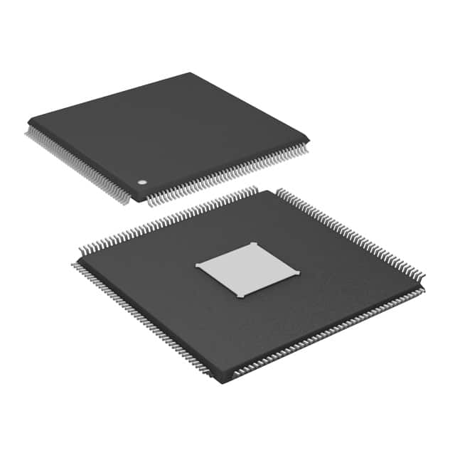
- Part No.:
- ADSP-BF512KSWZ-4
- Manufacturer:
- Analog Devices Inc.
- Category:
- DSP (Digital Signal Processors)
- Package:
- 176-LQFP Exposed Pad
- Datasheet:
-
 ADSP-BF512KSWZ-4.pdf
- Description:
- IC DSP 16/32B 400MHZ LP 176LQFP
- Quantity:
- Payment:

- Shipping:

Inventory:2,311
Please send an inquiry. Send us your inquiry, and we will respond immediately.
Product details
Overview
ADSP-BF512KSWZ-4 from Analog Devices is a 400 MHz Blackfin embedded processor with dual 16-bit MACs, 116 KB on-chip memory (32 KB L1 instruction SRAM, 32 KB L1 data SRAM, 4 KB scratchpad), and 40 GPIOs. It supports glueless SDRAM and asynchronous memory interfaces, features an on-chip PLL, and targets industrial control and motor drive applications requiring deterministic real-time signal processing.
For engineers reviewing the ADSP-BF512KSWZ-4 datasheet, ADSP-BF512KSWZ-4 pinout, ADSP-BF512KSWZ-4 application, or ADSP-BF512KSWZ-4 equivalent, key selection criteria include its 176-lead LQFP_EP package with exposed pad, absence of integrated Ethernet MAC or SPI flash, and compatibility with Blackfin toolchain and VisualDSP++ development environment.
Technical Context
The ADSP-BF512KSWZ-4 implements the Blackfin Micro Signal Architecture (MSA) with a modified Harvard memory system: separate 32 KB L1 instruction SRAM and 32 KB L1 data SRAM, both operating at full core speed, plus 4 KB dedicated scratchpad SRAM. Its dual-MAC, dual-ALU compute engine executes 16-bit × 16-bit multiplies per cycle with 40-bit accumulation and supports SIMD video operations.
It integrates a 56-input event handler with nested prioritized interrupts, 12 peripheral DMA channels (including SPORT, SPI, UART, PPI), and two memory-to-memory DMA controllers. The processor lacks IEEE 802.3 Ethernet MAC and on-die 16 Mbit SPI flash-features present only in BF518/BF518F16 and BF514F16/BF518F16 variants respectively-confirming its role as a cost-optimized, non-networked signal-processing node.
Key Specifications
| Parameter | Value and Actual Design Meaning |
|---|---|
| Core Speed | 400 MHz maximum operation-enables real-time execution of complex control loops and audio/video algorithms without external acceleration. |
| L1 Instruction Memory | 32 KB SRAM-provides zero-wait-state instruction fetch for deterministic timing-critical code sections. |
| L1 Data Memory | 32 KB SRAM-supports dual-access data buffers for simultaneous read/write in FFT or filter pipelines. |
| Scratchpad RAM | 4 KB dedicated SRAM-holds stack frames and local variables with guaranteed latency, isolated from cache coherency overhead. |
| External Memory Interface | Glueless 16-bit EBIU supporting SDRAM and asynchronous memories-eliminates address latching logic and reduces BOM count for memory expansion. |
| GPIO Count | 40 general-purpose I/O pins-sufficient for direct interface to encoders, sensors, PWM outputs, and status LEDs in motor control systems. |
| Package | 176-lead LQFP_EP with exposed thermal pad-enables high-power dissipation in industrial temperature range (−40°C to +85°C) without heatsink. |
Pinout & Package
ADSP-BF512KSWZ-4 is housed in a 176-lead LQFP_EP (exposed pad) package measuring 24 mm × 24 mm × 1.6 mm, qualified for industrial temperature operation. Pin assignments follow the standard ADSP-BF51x LQFP_EP lead assignment documented in Analog Devices Rev. D datasheet page 59.
| Pin/Terminal | Circuit Role | Design Meaning |
|---|---|---|
| VDDINT | Core power supply | 1.2 V ±3% input-powers processor core and L1 memory; requires low-noise regulation due to high-frequency switching current. |
| VDDEXT | I/O power supply | 3.3 V ±5% input-supplies all digital I/O banks including GPIO, SPI, UART, and PPI; enables mixed-voltage interfacing. |
| RESET | Active-low reset input | Asynchronous hard reset-asserted to initialize core state, clear registers, and force boot sequence from configured source (SPI/OTP/external). |
| CLKIN | External clock input | Accepts 1–50 MHz crystal or oscillator-feeds on-chip PLL to generate internal 400 MHz core clock and derived peripheral clocks. |
| BOOT_CFG[2:0] | Boot mode configuration | Three-pin strapping inputs-determine boot source (SPI flash, OTP, parallel memory, or host UART/SPI) at power-up. |
| PG11–PG14 | SPI0 interface signals | SPI0SS, SPI0SCK, SPI0MOSI, SPI0MISO-dedicated quad-line SPI port for external flash, sensors, or configuration EEPROM. |
Key Features
| Feature | Design Value |
|---|---|
| Dual 16-bit MAC + 40-bit ALUs | Enables concurrent multiply-accumulate and arithmetic operations per cycle-critical for real-time FIR/IIR filtering and motor FOC calculations. |
| Memory Management Unit (MMU) | Provides hardware-enforced memory protection between tasks-allows safe coexistence of RTOS kernel, application code, and device drivers in safety-aware systems. |
| 12 Peripheral DMA Channels | Offloads data movement from CPU for PPI video capture, SPORT audio streaming, and UART telemetry-reduces core utilization below 5% during sustained I/O. |
| 3-Phase 16-bit Center-Based PWM | Generates synchronized, dead-time-adjustable PWM pairs for 3-phase inverter control-directly drives gate drivers in BLDC/PMSM motor drives. |
| On-Chip PLL with Frequency Multiplication | Derives precise 400 MHz core clock from low-frequency crystal-eliminates need for external clock generator and simplifies board layout. |
Applications
| Industrial Motor Control | Audio Signal Processing |
|---|---|
Use Scenario: Closed-loop field-oriented control (FOC) of 3-phase BLDC motors in HVAC compressors and industrial pumps. IC Role / Device Role / Timing Role: Real-time execution of Park/Clarke transforms, PI current regulators, and space-vector PWM generation at 20 kHz switching frequency. Use Value: Deterministic 400 MHz core ensures sub-1 μs interrupt latency and jitter-free PWM output-prevents torque ripple and acoustic noise in precision motion systems. |
Use Scenario: Multi-channel audio effects processing (reverb, EQ, compression) in professional mixer consoles and broadcast equipment. IC Role / Device Role / Timing Role: Dual-SPI-connected ADC/DAC interface via PPI and SPORTs, with 32 KB L1 data SRAM buffering interleaved stereo samples. Use Value: Dual-MAC architecture processes 128-point FFTs in <10 μs-enables real-time spectral analysis and adaptive filtering without external DSP offload. |
| Embedded Vision Preprocessing | Secure Industrial Gateway |
Use Scenario: Edge-based image enhancement (noise reduction, edge sharpening) in smart cameras for factory floor inspection. IC Role / Device Role / Timing Role: Parallel peripheral interface (PPI) ingests raw ITU-R BT.656 video data; 4 video ALUs accelerate pixel-level operations. Use Value: Hardware-accelerated 8-bit average and SAA instructions reduce frame preprocessing time by 4× versus generic ARM Cortex-M-enabling 60 fps operation at VGA resolution. |
Use Scenario: Secure firmware update and device authentication in IIoT gateways connecting legacy Modbus/RS485 devices to cloud platforms. IC Role / Device Role / Timing Role: One-time programmable (OTP) memory stores cryptographic keys; Lockbox secure technology enforces code integrity verification at boot. Use Value: On-chip OTP and secure boot prevent unauthorized firmware modification-meets IEC 62443-3-3 SL2 requirements for industrial cybersecurity certification. |
Equivalent & Alternatives
The following parts are listed as comparable options for similar embedded signal processing applications.
| Alternative Part | Technical Difference | Application Difference | Selection Advice |
|---|---|---|---|
| ADSP-BF514KSWZ-4 | Includes RSI controller for SD/SDIO/MMC cards; same core, memory, and peripherals otherwise. | Required when local removable storage (e.g., firmware logging to microSD) is needed alongside motor control. | Select ADSP-BF514KSWZ-4 only if RSI interface is mandatory; otherwise ADSP-BF512KSWZ-4 offers lower cost and identical real-time performance. |
| ADSP-BF516KSWZ-4 | Integrates IEEE 802.3-compliant 10/100 Ethernet MAC; no SPI flash or RSI; same L1 memory map and GPIO count. | Suitable for networked industrial controllers requiring deterministic Ethernet I/O (e.g., EtherCAT slave nodes). | Choose ADSP-BF516KSWZ-4 when wired industrial Ethernet connectivity is required; ADSP-BF512KSWZ-4 remains optimal for standalone, non-networked edge processing. |
Compared with ADSP-BF514KSWZ-4 and ADSP-BF516KSWZ-4, the ADSP-BF512KSWZ-4 provides the minimal Blackfin feature set-omitting RSI and Ethernet-making it the most cost-effective choice for closed-loop control and signal processing where those interfaces are unused, while retaining full code compatibility and identical real-time determinism.
Availability
ADSP-BF512KSWZ-4 is available at Aetrix Electronics and suitable for industrial motor control, audio signal processing, embedded vision preprocessing, and secure industrial gateway applications requiring stable component supply across extended product lifecycles.
Supply support for ADSP-BF512KSWZ-4 includes scheduled delivery planning, volume procurement assistance, BOM continuity management, traceable sourcing, and lifecycle availability coordination for OEM customers, industrial embedded developers, connected-device designers, and electronics production programs.
Manufacturer
Analog Devices, Inc. is a global semiconductor leader specializing in high-performance analog, mixed-signal, and digital signal processing technologies for industrial, automotive, and communications markets.
The ADSP-BF512KSWZ-4 belongs to the Blackfin family-a line of embedded processors designed for applications demanding real-time signal processing, deterministic control, and low-power operation in resource-constrained environments.
FAQ
What is the maximum operating frequency of the ADSP-BF512KSWZ-4?
The ADSP-BF512KSWZ-4 operates at a maximum frequency of 400 MHz, achieved via its on-chip PLL multiplying a 1–50 MHz external clock input. This speed is fully supported across the industrial temperature range (−40°C to +85°C) and enables sub-microsecond interrupt response times critical for motor control and audio processing. All timing specifications in the Rev. D datasheet assume this 400 MHz operation.
Does the ADSP-BF512KSWZ-4 include integrated Ethernet or SPI flash memory?
No, the ADSP-BF512KSWZ-4 does not include an integrated IEEE 802.3 Ethernet MAC or on-die SPI flash memory. These features are exclusive to other members of the BF51x family: Ethernet appears only in BF516/BF518 variants, and 16 Mbit SPI flash is present solely in BF514F16 and BF518F16 models. The ADSP-BF512KSWZ-4 relies on external memory and communication interfaces.
What package type and thermal characteristics does the ADSP-BF512KSWZ-4 use?
The ADSP-BF512KSWZ-4 uses a 176-lead LQFP_EP package with an exposed thermal pad, measuring 24 mm × 24 mm × 1.6 mm. Its θJA is 26.5°C/W and θJC is 3.5°C/W (junction-to-case, top side), enabling reliable operation up to 85°C ambient when the exposed pad is soldered to a minimum 400 mm² copper pour. This package is explicitly qualified for industrial applications.
How does the memory architecture of the ADSP-BF512KSWZ-4 support real-time processing?
The ADSP-BF512KSWZ-4 employs a hierarchical memory architecture with 32 KB L1 instruction SRAM, 32 KB L1 data SRAM, and 4 KB scratchpad SRAM-all operating at full 400 MHz core speed with zero wait states. This eliminates cache misses and memory bottlenecks during tight control loops. The MMU further isolates memory regions to prevent task interference, ensuring predictable timing for safety-critical functions.
Is the ADSP-BF512KSWZ-4 pin-compatible with other BF51x processors?
Yes, the ADSP-BF512KSWZ-4 shares identical pinout and package dimensions with ADSP-BF514KSWZ-4, ADSP-BF516KSWZ-4, and ADSP-BF518KSWZ-4 in the 176-lead LQFP_EP variant. This allows hardware reuse across designs-e.g., upgrading from ADSP-BF512KSWZ-4 to ADSP-BF516KSWZ-4 requires only firmware and minor schematic changes for Ethernet PHY interface, with no PCB redesign needed.
ADSP-BF512KSWZ-4 Specifications
- Product attributes
- Attribute value
- Manufacturer:
- Analog Devices Inc.
- Series:
- Blackfin®
- Package/Case:
- 176-LQFP Exposed Pad
- Packaging:
- Tray
- Product Status:
- Active
- Type:
- Fixed Point
- Interface:
- I2C, PPI, SPI, SPORT, UART/USART
- Clock Rate:
- 400MHz
- Non-Volatile Memory:
- External
- On-Chip RAM:
- 116kB
- Voltage - I/O:
- 1.8V, 2.5V, 3.3V
- Voltage - Core:
- 1.30V
- Operating Temperature:
- 0°C ~ 70°C (TA)
- Grade:
- -
- Qualification:
- -
- Mounting Type:
- Surface Mount
- Supplier Device Package:
- 176-LQFP-EP (24x24)
ADSP-BF512KSWZ-4 FAQ
1.How can I place an order for ADSP-BF512KSWZ-4 through Aetrix?
Please submit a Request for Quotation (RFQ) for ADSP-BF512KSWZ-4 on Aetrix. Our sales agent will provide a competitive quotation and guide you through the order confirmation once you accept the terms.
2.Are the price and stock information for ADSP-BF512KSWZ-4 reliable?
The price and inventory of ADSP-BF512KSWZ-4 are updated periodically and may fluctuate due to market conditions. Stock and pricing data are typically refreshed every 24 hours. Quotation validity for ADSP-BF512KSWZ-4 is usually 5 days.
3.What payment methods are accepted for ADSP-BF512KSWZ-4?
We accept Wire Transfer, PayPal, Credit Card, Western Union, MoneyGram, and Escrow for ADSP-BF512KSWZ-4 transactions.
Note: Certain payment methods may incur a processing fee.
4.How is shipping managed for ADSP-BF512KSWZ-4?
ADSP-BF512KSWZ-4 orders can be shipped via leading logistics carriers, including DHL, UPS, FedEx, TNT, or Registered Mail.
Once your ADSP-BF512KSWZ-4 order is processed, you will receive an email with the shipment details and tracking number.
Note: Tracking information may take up to 24 hours to appear. Express delivery typically takes 3–5 business days.
5.How can I obtain technical support or documentation for ADSP-BF512KSWZ-4?
For technical support, including ADSP-BF512KSWZ-4 datasheets, pinout diagrams, or application guidance, please contact our engineering support team. They can provide detailed documentation and assistance for your ADSP-BF512KSWZ-4 requirements.
6.How does Aetrix verify that ADSP-BF512KSWZ-4 is sourced from the original manufacturer or authorized distributors?
All ADSP-BF512KSWZ-4 products on Aetrix are procured from qualified distributors and authorized channels. Our dedicated quality assurance team conducts strict verification, including traceability checks and, if necessary, third-party testing. This ensures that ADSP-BF512KSWZ-4 meets industry standards.
7.What is the process for return or replacement of ADSP-BF512KSWZ-4?
All ADSP-BF512KSWZ-4 units undergo pre-shipment inspection (PSI). If there is an issue with ADSP-BF512KSWZ-4, returns or replacements are accepted under the following conditions:
1.Quantity discrepancies, incorrect items, or visible external defects (such as breakage or corrosion), acknowledged by Aetrix.
2.The issue is reported within 90 days of delivery.
3.The ADSP-BF512KSWZ-4 part is unused and in its original packaging.
Return procedure for ADSP-BF512KSWZ-4:
1.Submit a request within 90 days.
2.Obtain a Return Material Authorization (RMA) from Aetrix.
ADSP-BF512KSWZ-4 Tags
-
TMS320C5535AZAY10
Texas Instruments
-
TMS320VC5501PGF300
Texas Instruments
-
ADSP-BF592KCPZ
Analog Devices Inc.
-
ADAU1463WBCPZ150
Analog Devices Inc.

-
TMS320VC5402PGE100
Texas Instruments

-
ADAU1701JSTZ-RL
Analog Devices Inc.
-
ADAU1701JSTZ
Analog Devices Inc.
-
TMS320VC5502PGF300
Texas Instruments
-
ADAU1462WBCPZ300RL
Analog Devices Inc.
-
ADAU1452KCPZRL
Analog Devices Inc.
-
ADAU1452WBCPZ-RL
Analog Devices Inc.
-
TMS320C6747DZKB3
Texas Instruments
Tech Hub

A practical engineering guide to 3.3V and 5V logic compatibility, input thresholds, resistor dividers, translator ICs, MOSFET level shifting, I2C pull-ups, timing limits and power-sequencing risks.

The 74HC595 uses push-pull logic outputs, while the TPIC6B595 uses 50 V open-drain DMOS sinks for higher-power loads. This guide compares timing, current limits, 3.3 V interfacing, load wiring, thermal…

The 74HC595 converts serial data into eight stable parallel outputs. This guide covers pin functions, shift and storage timing, OE and MR behavior, drive-current limits, cascading, voltage compatibilit…

A technical comparison of level-sensitive latches and edge-triggered flip-flops, covering timing windows, setup and hold limits, master–slave operation, time borrowing, race-through, HDL inference and…

A D latch stores one bit while Enable controls when data can pass. This reference covers gate-level operation, truth tables, transparency, setup and hold timing, LE versus OE, common ICs and practical …

An SR latch stores one bit through cross-coupled feedback. This engineering reference covers NOR and NAND implementations, truth tables, forbidden-state recovery, gated operation, switch debouncing, fa…

Latch circuits retain one bit through feedback. This technical reference covers SR and D latches, truth tables, transparency, timing limits, latch-versus-flip-flop behavior, applications and common log…

An engineering guide to LED driver operation, constant-current and constant-voltage outputs, linear and switching topologies, dimming, IC selection, calculations, replacement compatibility, and fault c…

Operational amplifier guide covering op amp basics, feedback, ideal vs real op amps, common configurations, buffer circuits, offset, bias current, gain-bandwidth, slew rate, rail-to-rail limits and sel…

Jumper cables guide covering safe connection order, red and black clamp placement, final ground connection, cable gauge, length, clamp quality, copper vs CCA cables, jump starter comparison and battery…


