
 My Inquiry
 My Account


Analog Devices Inc. ADSP-BF535PKB-350
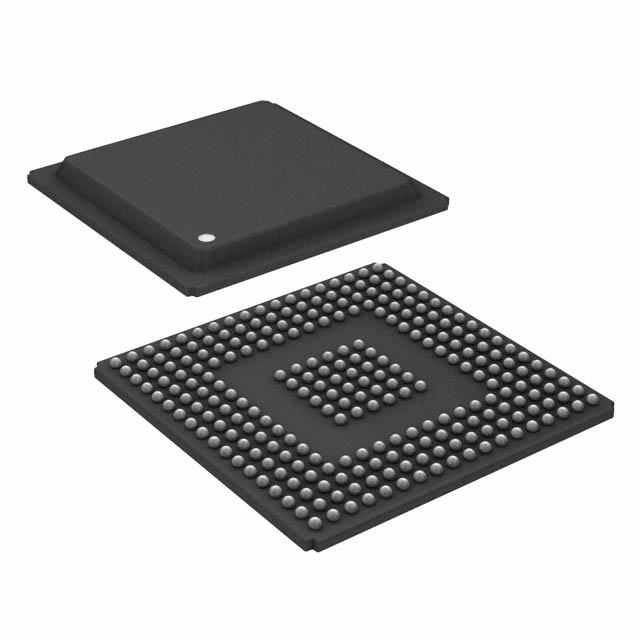
- Part No.:
- ADSP-BF535PKB-350
- Manufacturer:
- Analog Devices Inc.
- Category:
- DSP (Digital Signal Processors)
- Package:
- 260-BBGA
- Datasheet:
-
 ADSP-BF535PKB-350.pdf
- Description:
- IC DSP CONTROLLER 16BIT 260 BGA
- Quantity:
- Payment:

- Shipping:

Inventory:3,736
Please send an inquiry. Send us your inquiry, and we will respond immediately.
Product details
Overview
ADSP-BF535PKB-350 from Analog Devices is a 350 MHz Blackfin embedded processor featuring dual 16-bit MACs, 256 KB on-chip L2 SRAM, PCI 2.2-compliant bus interface, USB 1.1 device port, and real-time clock - deployed in portable digital communication appliances requiring integrated signal processing and system control.
For engineers reviewing the ADSP-BF535PKB-350 datasheet, ADSP-BF535PKB-350 pinout, ADSP-BF535PKB-350 application, or ADSP-BF535PKB-350 equivalent, key selection criteria include core clock speed, on-chip memory hierarchy (L1/L2 SRAM configuration), PCI/USB peripheral support, dynamic power management modes, and 260-ball PBGA package compatibility with high-density routing constraints.
Technical Context
The ADSP-BF535PKB-350 implements a modified Harvard architecture with hierarchical memory: 16 KB L1 instruction SRAM/cache, two 16 KB L1 data SRAM/cache banks, 4 KB scratch pad SRAM, and 256 KB unified L2 SRAM - all accessible at full 350 MHz core speed. Its dual-MAC, quad-video-ALU signal processing engine executes 16-/32-bit instructions with zero-overhead looping and SIMD multimedia acceleration.
Peripherals are tightly coupled via high-bandwidth internal buses: a 32-bit, 33 MHz PCI 2.2 interface supports both host and target roles; USB 1.1 operates in device-only mode; two full-duplex SPORTs and two SPI ports enable audio/modem codec interfacing; and four timers (three with PWM) plus programmable flag I/O provide real-time control. All peripherals except RTC, watchdog, and flags support dedicated DMA channels.
Key Specifications
| Parameter | Value and Actual Design Meaning |
|---|---|
| Core Frequency | 350 MHz - enables real-time execution of complex DSP algorithms (e.g., multi-channel audio codecs) within strict latency budgets. |
| L1 Memory | 16 KB instruction + 32 KB data SRAM/cache - provides deterministic low-latency access for critical code and data without external memory wait states. |
| L2 Memory | 256 KB unified SRAM - serves as high-bandwidth working memory for large buffers, FFT tables, or firmware images, eliminating SDRAM access bottlenecks. |
| PCI Interface | 32-bit, 33 MHz, PCI 2.2 compliant - allows glueless expansion with standard peripherals (e.g., Ethernet controllers, FPGA co-processors) in host or target configurations. |
| USB Interface | USB 1.1 device-only - supports direct connection to PCs for firmware updates, data logging, or host-controlled operation without external transceivers. |
| Power Management | 1.0–1.6 V core VDD with four operating modes (Full On, Active, Sleep, Deep Sleep) - enables battery life optimization in portable applications via voltage/frequency scaling. |
| Package | 260-ball PBGA (17 mm × 17 mm, 1.0 mm pitch) - supports high I/O count in compact footprint while maintaining thermal performance for sustained 350 MHz operation. |
Pinout & Package
ADSP-BF535PKB-350 is housed in a 260-ball plastic ball grid array (PBGA) package with 1.0 mm ball pitch and 17 mm × 17 mm body size. Thermal and mechanical specifications comply with JEDEC MO-218AB.
| Pin/Terminal | Circuit Role | Design Meaning |
|---|---|---|
| VDDINT | Core Power Supply | 1.0–1.6 V supply for processor core; requires tight regulation and local decoupling to sustain 350 MHz operation. |
| VDDIO | I/O Power Supply | 3.3 V supply for all digital I/Os (PCI, USB, SPORT, SPI, UART); tolerant of standard logic-level peripherals. |
| CLKIN | External Clock Input | Accepts 1–50 MHz crystal or oscillator input; feeds on-chip PLL with 1×–31× multiplier for generating 350 MHz core clock. |
| RESET | Active-Low Reset Input | Asynchronous reset signal; initiates boot sequence from on-chip ROM or configured external memory source. |
| BOOT[3:0] | Boot Configuration Pins | Four-pin strap determines boot source (ROM, SPI flash, parallel flash, or external SDRAM) at power-up. |
| PCI_AD[31:0] | PCI Address/Data Multiplexed Bus | 32-bit multiplexed address/data lines for PCI 2.2 interface; supports 132 MB/s peak bandwidth in 33 MHz mode. |
| USB_DP / USB_DM | USB Differential Data Lines | Full-speed (12 Mbps) USB 1.1 differential pair; requires 27 Ω series termination and 1.5 kΩ pull-up on DP for device enumeration. |
Key Features
| Feature | Design Value |
|---|---|
| Dual 16-bit MAC + Quad Video ALUs | Enables concurrent execution of two 16×16 multiply-accumulate operations per cycle plus video-specific arithmetic (e.g., motion estimation, chroma subsampling) without CPU intervention. |
| Memory Management Unit (MMU) | Provides hardware-enforced memory protection across tasks and prevents unauthorized access to system registers - essential for RTOS-based secure embedded systems. |
| Glueless External Memory Controllers | Integrates PC133 SDRAM and asynchronous memory controllers - eliminates external logic for interfacing up to 512 MB SDRAM and 256 MB flash/SRAM, reducing BOM cost and PCB area. |
| Zero-Overhead Looping | Hardware-accelerated loop control eliminates branch penalties for tight DSP loops (e.g., FIR filters), improving instruction throughput by up to 30% versus software-managed loops. |
| Flexible Event Handling Architecture | Two-stage interrupt controller (SIC + CEC) with nested, prioritized interrupts and configurable vector mapping - ensures deterministic response to real-time events (e.g., SPORT DMA completion, timer PWM edge). |
Applications
| VoIP Terminal Baseband Processing | Industrial HMI Controller |
|---|---|
Use Scenario: Real-time encoding/decoding of G.729/G.711 voice streams with echo cancellation and DTMF detection in compact SIP phones. IC Role / Device Role / Timing Role: Primary baseband processor executing DSP kernels, managing USB HID interface for keypad/display, and synchronizing audio sampling via SPORTs. Use Value: 350 MHz core + dual MACs deliver >200 MIPS sustained throughput for concurrent voice channels; 256 KB L2 SRAM stores codec coefficients and packet buffers without external memory latency. |
Use Scenario: Local operator interface for PLC-based machinery with touch screen, alarm logging, and fieldbus gateway functions. IC Role / Device Role / Timing Role: System-on-chip controller running RTOS, driving LCD via GPIO/SPORT, polling sensors via SPI, and bridging Modbus RTU over UART to EtherNet/IP via PCI-connected Ethernet MAC. Use Value: Integrated PCI and dual UARTs eliminate interface ICs; dynamic power management extends uptime in fanless enclosures; L1 cache ensures deterministic UI response under load. |
| Portable Medical Imaging Display | Automotive Infotainment Gateway |
Use Scenario: Battery-powered ultrasound display unit rendering B-mode images and overlaying measurement annotations in real time. IC Role / Device Role / Timing Role: Image processing engine performing scan conversion and contrast enhancement, coordinating frame capture via SPORT-connected ADC, and updating TFT display through programmable flag-driven timing signals. Use Value: 40-bit accumulators prevent precision loss in multi-stage filtering; 1.0 V core voltage minimizes active power draw; 260-ball PBGA fits constrained medical enclosure layouts. |
Use Scenario: In-vehicle head unit aggregating audio sources (Bluetooth A2DP, USB media, FM tuner) and routing to amplifier via I²S, while managing CAN diagnostics and OTA updates. IC Role / Device Role / Timing Role: Central multimedia processor handling audio decoding, USB mass storage, and CAN message filtering - using UART for diagnostic debug and PCI for legacy ASIC co-processing. Use Value: USB 1.1 device port enables secure firmware updates via service laptop; programmable flags implement custom CAN wake-up signaling; L2 SRAM caches audio decode buffers for glitch-free playback. |
Equivalent & Alternatives
The following parts are listed as comparable options for similar embedded signal processing applications.
| Alternative Part | Technical Difference | Application Difference | Selection Advice |
|---|---|---|---|
| ADSP-BF533KCPZ-500 | 500 MHz core, 136-ball CSP package, no PCI interface, reduced L2 SRAM (64 KB), same L1 memory map. | Better suited for space-constrained, high-MIPS-only applications (e.g., motor control) where PCI expansion is unnecessary. | Select when maximum computational throughput in minimal footprint is required and PCI/USB device functionality is not needed. |
| ADSP-BF537KBCZ-500 | 500 MHz core, 256-ball PBGA, adds EMAC (10/100 Ethernet MAC), retains PCI and USB, same memory hierarchy. | Targeted at networked embedded systems requiring wired Ethernet connectivity alongside PCI expansion and USB device capability. | Choose when integrating native Ethernet with existing PCI/USB infrastructure - avoids external PHY and reduces layer-2 protocol stack overhead. |
Compared with ADSP-BF535PKB-350, the BF533 offers higher clock speed in smaller package but sacrifices PCI and half the L2 SRAM; the BF537 adds Ethernet MAC at same package size and frequency, enabling network-aware designs without external MAC chips - both require revalidation of power delivery and thermal design due to different voltage/current profiles.
Availability
ADSP-BF535PKB-350 is available at Aetrix Electronics and suitable for portable digital communication appliances, industrial human-machine interfaces, and battery-powered medical imaging displays requiring stable component supply across extended production lifecycles.
Supply support for ADSP-BF535PKB-350 includes scheduled delivery planning, volume procurement assistance, BOM continuity management, traceable sourcing, and lifecycle availability coordination for OEM customers, industrial embedded developers, connected-device designers, and electronics production programs.
Manufacturer
Analog Devices, Inc. is a global leader in high-performance analog, mixed-signal, and digital signal processing semiconductors, headquartered in Norwood, MA, with design centers worldwide and ISO 9001-certified manufacturing.
The ADSP-BF535PKB-350 belongs to the Blackfin family - engineered for applications demanding combined general-purpose control and real-time signal processing in low-power, highly integrated SoC form factors, especially portable and embedded communications equipment.
FAQ
What is the maximum operating frequency of the ADSP-BF535PKB-350?
The ADSP-BF535PKB-350 is rated for a maximum core clock frequency of 350 MHz, achieved using its on-chip PLL with programmable multiplication factor (1× to 31×) driven by an external 1–50 MHz reference clock. This frequency is guaranteed across the commercial temperature range (0°C to 70°C) with proper 1.0–1.6 V core supply regulation and thermal management.
Does the ADSP-BF535PKB-350 support booting from external flash memory?
Yes, the ADSP-BF535PKB-350 supports booting from external parallel flash memory via its asynchronous memory controller. Boot mode is selected by strapping BOOT[3:0] pins at power-up; configuration 0x01 (BOOT3=0, BOOT2=0, BOOT1=0, BOOT0=1) enables boot from async memory bank 0, allowing execution directly from flash without copying to RAM.
Can the ADSP-BF535PKB-350 operate as a PCI bus master?
Yes, the ADSP-BF535PKB-350 supports full PCI 2.2 master and slave functionality. As a master, it can initiate transactions to configure and communicate with other PCI devices; as a slave, it responds to accesses from a host CPU. Both modes use the same 32-bit, 33 MHz interface with dedicated configuration, I/O, and memory address spaces mapped into the processor's 4 GB address space.
What type of USB interface does the ADSP-BF535PKB-350 provide?
The ADSP-BF535PKB-350 integrates a USB 1.1-compliant device-only interface - it cannot function as a USB host. The interface supports full-speed (12 Mbps) operation with built-in transceiver, requiring only external 27 Ω series resistors and a 1.5 kΩ pull-up resistor on USB_DP for enumeration as a standard USB device (e.g., CDC ACM, HID, or vendor-specific class).
How much on-chip memory does the ADSP-BF535PKB-350 have, and how is it organized?
The ADSP-BF535PKB-350 contains 308 KB of on-chip memory: 16 KB L1 instruction SRAM/cache, two 16 KB L1 data SRAM/cache banks (32 KB total), 4 KB L1 scratch pad SRAM, and 256 KB unified L2 SRAM. L1 memories operate at full core speed with configurable cache/SRAM modes; L2 SRAM provides high-bandwidth unified code/data storage with slightly higher latency than L1.
ADSP-BF535PKB-350 Specifications
- Product attributes
- Attribute value
- Manufacturer:
- Analog Devices Inc.
- Series:
- Blackfin®
- Package/Case:
- 260-BBGA
- Packaging:
- Tray
- Product Status:
- Obsolete
- Type:
- Fixed Point
- Interface:
- PCI, SPI, SSP, UART, USB
- Clock Rate:
- 350MHz
- Non-Volatile Memory:
- External
- On-Chip RAM:
- 308kB
- Voltage - I/O:
- 3.30V
- Voltage - Core:
- 1.60V
- Operating Temperature:
- 0°C ~ 70°C (TA)
- Grade:
- -
- Qualification:
- -
- Mounting Type:
- Surface Mount
- Supplier Device Package:
- 260-PBGA (19x19)
ADSP-BF535PKB-350 FAQ
1.How can I place an order for ADSP-BF535PKB-350 through Aetrix?
Please submit a Request for Quotation (RFQ) for ADSP-BF535PKB-350 on Aetrix. Our sales agent will provide a competitive quotation and guide you through the order confirmation once you accept the terms.
2.Are the price and stock information for ADSP-BF535PKB-350 reliable?
The price and inventory of ADSP-BF535PKB-350 are updated periodically and may fluctuate due to market conditions. Stock and pricing data are typically refreshed every 24 hours. Quotation validity for ADSP-BF535PKB-350 is usually 5 days.
3.What payment methods are accepted for ADSP-BF535PKB-350?
We accept Wire Transfer, PayPal, Credit Card, Western Union, MoneyGram, and Escrow for ADSP-BF535PKB-350 transactions.
Note: Certain payment methods may incur a processing fee.
4.How is shipping managed for ADSP-BF535PKB-350?
ADSP-BF535PKB-350 orders can be shipped via leading logistics carriers, including DHL, UPS, FedEx, TNT, or Registered Mail.
Once your ADSP-BF535PKB-350 order is processed, you will receive an email with the shipment details and tracking number.
Note: Tracking information may take up to 24 hours to appear. Express delivery typically takes 3–5 business days.
5.How can I obtain technical support or documentation for ADSP-BF535PKB-350?
For technical support, including ADSP-BF535PKB-350 datasheets, pinout diagrams, or application guidance, please contact our engineering support team. They can provide detailed documentation and assistance for your ADSP-BF535PKB-350 requirements.
6.How does Aetrix verify that ADSP-BF535PKB-350 is sourced from the original manufacturer or authorized distributors?
All ADSP-BF535PKB-350 products on Aetrix are procured from qualified distributors and authorized channels. Our dedicated quality assurance team conducts strict verification, including traceability checks and, if necessary, third-party testing. This ensures that ADSP-BF535PKB-350 meets industry standards.
7.What is the process for return or replacement of ADSP-BF535PKB-350?
All ADSP-BF535PKB-350 units undergo pre-shipment inspection (PSI). If there is an issue with ADSP-BF535PKB-350, returns or replacements are accepted under the following conditions:
1.Quantity discrepancies, incorrect items, or visible external defects (such as breakage or corrosion), acknowledged by Aetrix.
2.The issue is reported within 90 days of delivery.
3.The ADSP-BF535PKB-350 part is unused and in its original packaging.
Return procedure for ADSP-BF535PKB-350:
1.Submit a request within 90 days.
2.Obtain a Return Material Authorization (RMA) from Aetrix.
ADSP-BF535PKB-350 Tags
-
TMS320C5535AZAY10
Texas Instruments
-
TMS320VC5501PGF300
Texas Instruments
-
ADSP-BF592KCPZ
Analog Devices Inc.
-
ADAU1463WBCPZ150
Analog Devices Inc.

-
TMS320VC5402PGE100
Texas Instruments

-
ADAU1701JSTZ-RL
Analog Devices Inc.
-
ADAU1701JSTZ
Analog Devices Inc.
-
TMS320VC5502PGF300
Texas Instruments
-
ADAU1462WBCPZ300RL
Analog Devices Inc.
-
ADAU1452KCPZRL
Analog Devices Inc.
-
ADAU1452WBCPZ-RL
Analog Devices Inc.
-
TMS320C6747DZKB3
Texas Instruments
Tech Hub

A practical engineering guide to 3.3V and 5V logic compatibility, input thresholds, resistor dividers, translator ICs, MOSFET level shifting, I2C pull-ups, timing limits and power-sequencing risks.

The 74HC595 uses push-pull logic outputs, while the TPIC6B595 uses 50 V open-drain DMOS sinks for higher-power loads. This guide compares timing, current limits, 3.3 V interfacing, load wiring, thermal…

The 74HC595 converts serial data into eight stable parallel outputs. This guide covers pin functions, shift and storage timing, OE and MR behavior, drive-current limits, cascading, voltage compatibilit…

A technical comparison of level-sensitive latches and edge-triggered flip-flops, covering timing windows, setup and hold limits, master–slave operation, time borrowing, race-through, HDL inference and…

A D latch stores one bit while Enable controls when data can pass. This reference covers gate-level operation, truth tables, transparency, setup and hold timing, LE versus OE, common ICs and practical …

An SR latch stores one bit through cross-coupled feedback. This engineering reference covers NOR and NAND implementations, truth tables, forbidden-state recovery, gated operation, switch debouncing, fa…

Latch circuits retain one bit through feedback. This technical reference covers SR and D latches, truth tables, transparency, timing limits, latch-versus-flip-flop behavior, applications and common log…

An engineering guide to LED driver operation, constant-current and constant-voltage outputs, linear and switching topologies, dimming, IC selection, calculations, replacement compatibility, and fault c…

Operational amplifier guide covering op amp basics, feedback, ideal vs real op amps, common configurations, buffer circuits, offset, bias current, gain-bandwidth, slew rate, rail-to-rail limits and sel…

Jumper cables guide covering safe connection order, red and black clamp placement, final ground connection, cable gauge, length, clamp quality, copper vs CCA cables, jump starter comparison and battery…


