
 My Inquiry
 My Account


Analog Devices Inc. ADSP-BF536BBCZ4BRL
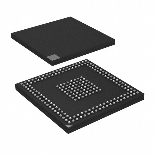
- Part No.:
- ADSP-BF536BBCZ4BRL
- Manufacturer:
- Analog Devices Inc.
- Category:
- DSP (Digital Signal Processors)
- Package:
- 208-FBGA, CSPBGA
- Datasheet:
-
 ADSP-BF536BBCZ4BRL.pdf
- Description:
- IC DSP CTLR 16BIT 208CSBGA
- Quantity:
- Payment:

- Shipping:

Inventory:1,323
Please send an inquiry. Send us your inquiry, and we will respond immediately.
Product details
Overview
ADSP-BF536BBCZ4BRL from Analog Devices is a Blackfin embedded processor with dual 16-bit MACs, 400 MHz maximum clock speed, 132 KB on-chip memory (including 16 KB instruction SRAM/cache, 32 KB data SRAM/cache, 32 KB dedicated data SRAM, and 4 KB scratchpad), and integrated CAN 2.0B, PPI, two SPORTs, two UARTs, SPI, TWI, eight 32-bit timers with PWM, RTC, and watchdog - deployed in industrial motor control and automotive body electronics.
For engineers reviewing the ADSP-BF536BBCZ4BRL datasheet, ADSP-BF536BBCZ4BRL pinout, ADSP-BF536BBCZ4BRL application, or ADSP-BF536BBCZ4BRL equivalent, key selection criteria include its 182-ball CSP_BGA package, IEEE 802.3-compliant 10/100 Ethernet MAC (present only in BF536/BF537), dynamic voltage/frequency scaling for power management, and full code-and-pin compatibility within the BF534/BF536/BF537 family.
Technical Context
The ADSP-BF536BBCZ4BRL implements a modified Harvard architecture with hierarchical L1 memory (instruction/data/scratchpad SRAM), MMU-based memory protection, and three operating modes (user/supervisor/emulation). Its core integrates two 40-bit ALUs, four 8-bit video ALUs, and a 40-bit shifter supporting SIMD multimedia operations.
Peripherals are connected via high-bandwidth buses up to 133 MHz, with flexible DMA routing: 12 peripheral DMAs (2 Ethernet-assigned) and 2 memory-to-memory DMAs. The event controller supports nested/prioritized interrupts across 32 inputs, managed by dual-stage CEC and SIC with configurable IAR mapping.
Key Specifications
| Parameter | Value and Actual Design Meaning |
|---|---|
| Core Architecture | Blackfin® dual-MAC, RISC-like instruction set with SIMD video ALUs and 40-bit shifter |
| Max Clock Speed | 400 MHz - determines real-time signal processing throughput and loop execution rate |
| On-Chip Memory | 132 KB total: 16 KB L1 instruction SRAM/cache + 48 KB L1 instruction SRAM + 32 KB L1 data SRAM/cache + 32 KB L1 data SRAM + 4 KB scratchpad SRAM |
| Package | 182-ball CSP_BGA - enables compact PCB layout with fine-pitch interconnect and thermal performance suitable for automotive and industrial enclosures |
| Ethernet MAC | IEEE 802.3-compliant 10/100 - provides native wired network connectivity without external PHY or glue logic |
| CAN Interface | CAN 2.0B - supports robust automotive bus communication with error handling and message filtering |
| Power Management | On-chip programmable voltage regulator with dynamic V/F scaling - reduces active power consumption in portable and battery-backed systems |
Pinout & Package
ADSP-BF536BBCZ4BRL is housed in an 182-ball CSP_BGA package (ball pitch: 0.5 mm, body size: 12 mm × 12 mm), qualified for automotive applications per AEC-Q100. Ball assignments follow the standardized layout defined in Analog Devices' Rev. J datasheet, Pages 57–59.
| Pin/Terminal | Circuit Role | Design Meaning |
|---|---|---|
| VDDINT | Core supply voltage input | Supplies regulated 1.2 V to processor core; requires local decoupling for noise-sensitive DSP operation |
| VDDIO | I/O supply voltage input | Supplies 3.3 V to all digital I/O banks; enables interface compatibility with standard logic families |
| CLKIN | External clock input | Accepts 1–50 MHz crystal or oscillator reference; feeds on-chip PLL for internal clock generation |
| RESET | Active-low reset input | Asynchronous hardware reset; initiates boot sequence from internal ROM or configured external source |
| BOOT_CFG[2:0] | Boot configuration pins | Determines boot source (SPI flash, TWI EEPROM, UART host, etc.) at power-up; latched on reset release |
| EMU | JTAG emulation test access | Enables boundary-scan, debug, and trace via standard 14-pin JTAG interface compliant with IEEE 1149.1 |
Key Features
| Feature | Design Value |
|---|---|
| Dual 16-bit MACs + 40-bit ALUs | Enables simultaneous multiply-accumulate and arithmetic operations for real-time FIR/IIR filtering and FFT kernels |
| Flexible boot options | Supports boot from SPI flash, TWI EEPROM, UART host, or internal ROM - simplifies field firmware updates and production programming |
| Memory Management Unit (MMU) | Provides task-level memory protection and privilege separation - essential for RTOS-based safety-critical applications |
| Parallel Peripheral Interface (PPI) | Supports ITU-R BT.656 video data formats - enables direct connection to CCD/CMOS image sensors in vision systems |
| Two dual-channel SPORTs | Handles 8 stereo I²S channels - allows concurrent audio capture/playback with low-latency DMA-driven streaming |
Applications
| Industrial Motor Control | Automotive Body Electronics |
|---|---|
Use Scenario: Real-time closed-loop control of BLDC motors in HVAC actuators and power seat modules. IC Role / Device Role / Timing Role: Primary controller executing PID algorithms, PWM generation, and CAN-based diagnostics. Use Value: On-chip 400 MHz processing, 8 PWM-capable timers, and CAN 2.0B reduce BOM count and enable deterministic sub-10 µs control loop timing. | Use Scenario: Central gateway node managing lighting, window lift, and mirror control via CAN and LIN subnets. IC Role / Device Role / Timing Role: System-on-chip host processor coordinating multi-protocol communication and local decision logic. Use Value: Integrated CAN, UART, TWI, and 48 GPIOs eliminate external protocol translators; 132 KB on-chip memory stores multiple firmware images and diagnostic logs. |
| Networked Audio Processing | Portable Medical Imaging |
Use Scenario: Multi-channel audio codec interfacing with MEMS microphones and Class-D amplifiers in VoIP endpoints. IC Role / Device Role / Timing Role: Signal processor handling echo cancellation, beamforming, and I²S audio streaming. Use Value: Dual SPORTs support 8 stereo I²S lanes; 40-bit accumulators ensure >96 dB SNR in fixed-point audio math without overflow. | Use Scenario: Ultrasound front-end subsystem capturing and preprocessing RF echo data from transducer arrays. IC Role / Device Role / Timing Role: Real-time DSP engine performing beamforming, filtering, and envelope detection prior to host transfer. Use Value: 132 KB on-chip SRAM buffers raw RF samples; PPI interface directly acquires digitized echo streams from ADCs at up to 65 MSPS. |
Equivalent & Alternatives
The following parts are listed as comparable options for similar embedded DSP processor applications.
| Alternative Part | Technical Difference | Application Difference | Selection Advice |
|---|---|---|---|
| ADSP-BF537BBCZ6 | 600 MHz max speed, identical 182-ball CSP_BGA package, same peripherals including Ethernet MAC and CAN | Higher compute bandwidth suits demanding radar or video analytics where BF536's 400 MHz is limiting | Select BF537 when algorithm latency or FFT throughput exceeds BF536 capability; verify thermal design for higher power dissipation |
| ADSP-BF536BBCZ-5 | Same 400 MHz speed and 182-ball CSP_BGA, but rated for industrial temperature range (−40°C to +85°C) vs. automotive (−40°C to +105°C) | Lacks AEC-Q100 qualification; unsuitable for under-hood or safety-critical vehicle domains | Choose BF536BBCZ-5 for cost-sensitive industrial HMI or test equipment where extended temperature is unnecessary |
Compared with ADSP-BF536BBCZ4BRL, ADSP-BF537BBCZ6 delivers 50% higher clock speed and computational headroom while maintaining pin and code compatibility, whereas ADSP-BF536BBCZ-5 trades automotive qualification for lower unit cost in non-automotive deployments - both preserve identical memory map, peripheral register layout, and toolchain support.
Availability
ADSP-BF536BBCZ4BRL is available at Aetrix Electronics and suitable for industrial motor control, automotive body electronics, networked audio processing, and portable medical imaging requiring stable component supply across long-life product cycles.
Supply support for ADSP-BF536BBCZ4BRL includes scheduled delivery planning, volume procurement assistance, BOM continuity management, traceable sourcing, and lifecycle availability coordination for OEM customers, industrial embedded developers, connected-device designers, and electronics production programs.
Manufacturer
Analog Devices, Inc. is a global leader in high-performance analog, mixed-signal, and DSP technology, headquartered in Norwood, MA, serving industrial, automotive, communications, and healthcare markets.
The ADSP-BF536BBCZ4BRL belongs to the Blackfin® embedded processor family, designed specifically for applications demanding real-time signal processing, deterministic control, and multi-protocol connectivity in resource-constrained environments.
FAQ
What is the maximum operating frequency of the ADSP-BF536BBCZ4BRL?
The ADSP-BF536BBCZ4BRL has a maximum clock speed of 400 MHz, verified in the Analog Devices ADSP-BF534/536/537 Rev. J datasheet (Page 3, Table 1). This speed defines the upper bound for instruction execution, MAC throughput, and real-time interrupt response. The processor achieves this using its on-chip PLL with external CLKIN reference, and thermal derating may apply under sustained load in high-ambient conditions. ADSP-BF536BBCZ4BRL operates reliably across the full automotive temperature range (−40°C to +105°C).
Does the ADSP-BF536BBCZ4BRL include an Ethernet MAC?
Yes, the ADSP-BF536BBCZ4BRL integrates an IEEE 802.3-compliant 10/100 Ethernet MAC, as confirmed in the "Peripherals" section (Page 1) and Table 1 (Page 3) of the Rev. J datasheet. It supports MII/RMII interfaces and includes dedicated DMA channels (DMAR1 for Rx, DMAR2 for Tx). Unlike the ADSP-BF534, the ADSP-BF536BBCZ4BRL includes this module - enabling standalone wired networking without external MAC or PHY components. ADSP-BF536BBCZ4BRL does not integrate a physical layer; an external PHY is required.
What memory configurations are available on the ADSP-BF536BBCZ4BRL?
The ADSP-BF536BBCZ4BRL provides 132 KB of on-chip memory: 16 KB L1 instruction SRAM/cache, 48 KB L1 instruction SRAM, 32 KB L1 data SRAM/cache, 32 KB L1 data SRAM, and 4 KB scratchpad SRAM - totaling 132 KB as stated in the "Memory" section (Page 1) and Table 1 (Page 3). All blocks operate at full core speed with zero wait states. The memory map is fixed and documented in Figure 3 (Pages 6–7); no runtime reconfiguration of cache/SRAM allocation is supported. ADSP-BF536BBCZ4BRL also supports external SDRAM (up to 512 MB) and asynchronous memory via its EBIU.
Is the ADSP-BF536BBCZ4BRL pin-compatible with other Blackfin processors?
Yes, the ADSP-BF536BBCZ4BRL is fully pin-compatible and code-compatible with the ADSP-BF534 and ADSP-BF537 in the same 182-ball CSP_BGA package variant, as explicitly stated in the "General Description" (Page 3): "The ADSP-BF534/ADSP-BF536/ADSP-BF537 processors are completely code and pin compatible." Pin assignments, ball-out mapping, and power sequencing requirements match exactly - enabling drop-in replacement during design iteration or qualification. ADSP-BF536BBCZ4BRL shares identical footprint, thermal pad layout, and JTAG interface definition with BF534/BF537 182-ball variants.
What development tools support the ADSP-BF536BBCZ4BRL?
The ADSP-BF536BBCZ4BRL is supported by Analog Devices' CrossCore Embedded Studio (CCES), legacy VisualDSP++ 5.0, and GNU-based toolchains (GCC, GDB). Hardware debugging uses standard JTAG via ICE-1000/2000 emulators or USB-based EZ-KIT Lite evaluation boards. Peripheral drivers, BSPs, and RTOS integrations (ThreadX, FreeRTOS) are provided in the Blackfin Software Development Kit (SDK). ADSP-BF536BBCZ4BRL-specific device support files and memory configuration templates are included in CCES v2.10.0+ and VisualDSP++ Update 10.
ADSP-BF536BBCZ4BRL Specifications
- Product attributes
- Attribute value
- Manufacturer:
- Analog Devices Inc.
- Series:
- Blackfin®
- Package/Case:
- 208-FBGA, CSPBGA
- Packaging:
- Tape & Reel (TR)
- Product Status:
- Active
- Type:
- Fixed Point
- Interface:
- CAN, SPI, SSP, TWI, UART
- Clock Rate:
- 400MHz
- Non-Volatile Memory:
- External
- On-Chip RAM:
- 100kB
- Voltage - I/O:
- 2.50V, 3.30V
- Voltage - Core:
- 1.20V
- Operating Temperature:
- -40°C ~ 85°C (TA)
- Grade:
- -
- Qualification:
- -
- Mounting Type:
- Surface Mount
- Supplier Device Package:
- 208-CSPBGA (17x17)
ADSP-BF536BBCZ4BRL FAQ
1.How can I place an order for ADSP-BF536BBCZ4BRL through Aetrix?
Please submit a Request for Quotation (RFQ) for ADSP-BF536BBCZ4BRL on Aetrix. Our sales agent will provide a competitive quotation and guide you through the order confirmation once you accept the terms.
2.Are the price and stock information for ADSP-BF536BBCZ4BRL reliable?
The price and inventory of ADSP-BF536BBCZ4BRL are updated periodically and may fluctuate due to market conditions. Stock and pricing data are typically refreshed every 24 hours. Quotation validity for ADSP-BF536BBCZ4BRL is usually 5 days.
3.What payment methods are accepted for ADSP-BF536BBCZ4BRL?
We accept Wire Transfer, PayPal, Credit Card, Western Union, MoneyGram, and Escrow for ADSP-BF536BBCZ4BRL transactions.
Note: Certain payment methods may incur a processing fee.
4.How is shipping managed for ADSP-BF536BBCZ4BRL?
ADSP-BF536BBCZ4BRL orders can be shipped via leading logistics carriers, including DHL, UPS, FedEx, TNT, or Registered Mail.
Once your ADSP-BF536BBCZ4BRL order is processed, you will receive an email with the shipment details and tracking number.
Note: Tracking information may take up to 24 hours to appear. Express delivery typically takes 3–5 business days.
5.How can I obtain technical support or documentation for ADSP-BF536BBCZ4BRL?
For technical support, including ADSP-BF536BBCZ4BRL datasheets, pinout diagrams, or application guidance, please contact our engineering support team. They can provide detailed documentation and assistance for your ADSP-BF536BBCZ4BRL requirements.
6.How does Aetrix verify that ADSP-BF536BBCZ4BRL is sourced from the original manufacturer or authorized distributors?
All ADSP-BF536BBCZ4BRL products on Aetrix are procured from qualified distributors and authorized channels. Our dedicated quality assurance team conducts strict verification, including traceability checks and, if necessary, third-party testing. This ensures that ADSP-BF536BBCZ4BRL meets industry standards.
7.What is the process for return or replacement of ADSP-BF536BBCZ4BRL?
All ADSP-BF536BBCZ4BRL units undergo pre-shipment inspection (PSI). If there is an issue with ADSP-BF536BBCZ4BRL, returns or replacements are accepted under the following conditions:
1.Quantity discrepancies, incorrect items, or visible external defects (such as breakage or corrosion), acknowledged by Aetrix.
2.The issue is reported within 90 days of delivery.
3.The ADSP-BF536BBCZ4BRL part is unused and in its original packaging.
Return procedure for ADSP-BF536BBCZ4BRL:
1.Submit a request within 90 days.
2.Obtain a Return Material Authorization (RMA) from Aetrix.
ADSP-BF536BBCZ4BRL Tags
-
TMS320C5535AZAY10
Texas Instruments
-
TMS320VC5501PGF300
Texas Instruments
-
ADSP-BF592KCPZ
Analog Devices Inc.
-
ADAU1463WBCPZ150
Analog Devices Inc.

-
TMS320VC5402PGE100
Texas Instruments

-
ADAU1701JSTZ-RL
Analog Devices Inc.
-
ADAU1701JSTZ
Analog Devices Inc.
-
TMS320VC5502PGF300
Texas Instruments
-
ADAU1462WBCPZ300RL
Analog Devices Inc.
-
ADAU1452KCPZRL
Analog Devices Inc.
-
ADAU1452WBCPZ-RL
Analog Devices Inc.
-
TMS320C6747DZKB3
Texas Instruments
Tech Hub

A practical engineering guide to 3.3V and 5V logic compatibility, input thresholds, resistor dividers, translator ICs, MOSFET level shifting, I2C pull-ups, timing limits and power-sequencing risks.

The 74HC595 uses push-pull logic outputs, while the TPIC6B595 uses 50 V open-drain DMOS sinks for higher-power loads. This guide compares timing, current limits, 3.3 V interfacing, load wiring, thermal…

The 74HC595 converts serial data into eight stable parallel outputs. This guide covers pin functions, shift and storage timing, OE and MR behavior, drive-current limits, cascading, voltage compatibilit…

A technical comparison of level-sensitive latches and edge-triggered flip-flops, covering timing windows, setup and hold limits, master–slave operation, time borrowing, race-through, HDL inference and…

A D latch stores one bit while Enable controls when data can pass. This reference covers gate-level operation, truth tables, transparency, setup and hold timing, LE versus OE, common ICs and practical …

An SR latch stores one bit through cross-coupled feedback. This engineering reference covers NOR and NAND implementations, truth tables, forbidden-state recovery, gated operation, switch debouncing, fa…

Latch circuits retain one bit through feedback. This technical reference covers SR and D latches, truth tables, transparency, timing limits, latch-versus-flip-flop behavior, applications and common log…

An engineering guide to LED driver operation, constant-current and constant-voltage outputs, linear and switching topologies, dimming, IC selection, calculations, replacement compatibility, and fault c…

Operational amplifier guide covering op amp basics, feedback, ideal vs real op amps, common configurations, buffer circuits, offset, bias current, gain-bandwidth, slew rate, rail-to-rail limits and sel…

Jumper cables guide covering safe connection order, red and black clamp placement, final ground connection, cable gauge, length, clamp quality, copper vs CCA cables, jump starter comparison and battery…


