
 My Inquiry
 My Account


Analog Devices Inc. ADSP-BF609BBCZ-5
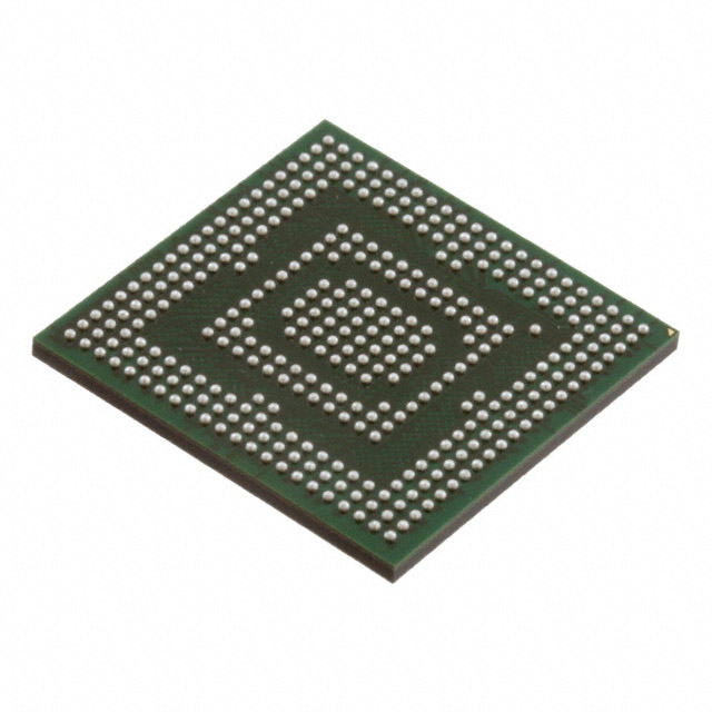
- Part No.:
- ADSP-BF609BBCZ-5
- Manufacturer:
- Analog Devices Inc.
- Category:
- DSP (Digital Signal Processors)
- Package:
- 349-LFBGA, CSPBGA
- Datasheet:
-
 ADSP-BF609BBCZ-5.pdf
- Description:
- IC DSP CTLR DUAL 349CSBGA
- Quantity:
- Payment:

- Shipping:

Inventory:3,327
Please send an inquiry. Send us your inquiry, and we will respond immediately.
Product details
Overview
ADSP-BF609BBCZ-5 from Analog Devices is a dual-core Blackfin embedded processor operating at up to 500 MHz per core, integrating two 16-bit MACs and two 40-bit ALUs per core, 256 KB of ECC-protected L2 SRAM, and a pipelined vision processor optimized for HD video pre- and co-processing in ADAS systems.
For engineers reviewing the ADSP-BF609BBCZ-5 datasheet, ADSP-BF609BBCZ-5 pinout, ADSP-BF609BBCZ-5 application, or ADSP-BF609BBCZ-5 equivalent, key selection criteria include dual-core deterministic real-time signal processing, hardware-accelerated vision pipeline support, IEEE 1588-compliant dual EMAC interfaces, and 349-ball CSP_BGA package compatibility with automotive-grade thermal and reliability requirements.
Technical Context
The ADSP-BF609BBCZ-5 implements a symmetric dual-core architecture with independent L1 instruction (64 KB) and data (32 KB) SRAM per core, each protected by multi-parity bits, and shares a unified 256 KB ECC-protected L2 SRAM domain accessible via a 64-bit bus at SYSCLK frequency.
Its system infrastructure includes a pipelined vision processor supporting HD-resolution (1280 × 960) frame processing, dual IEEE 1588 Ethernet MACs, 3× PPI, 4× link ports, 1× CAN 2.0B interface, and a trigger routing unit enabling autonomous DMA sequencing without CPU intervention.
Key Specifications
| Parameter | Value and Actual Design Meaning |
|---|---|
| Core Count & Speed | Dual Blackfin cores, each up to 500 MHz - enables parallel real-time signal and control tasks with deterministic latency. |
| L1 Memory per Core | 64 KB instruction + 32 KB data SRAM with multi-parity protection - ensures high-speed, fault-resilient core-local code and data execution. |
| L2 Memory | 256 KB unified SRAM with ECC protection - provides shared, error-corrected memory space for inter-core communication and large buffers. |
| Vision Processing | Pipelined Vision Processor (PVP) supporting HD resolution (1280 × 960) - offloads pixel-level video preprocessing from CPU cores in ADAS camera systems. |
| Peripheral Interfaces | Dual IEEE 1588 Ethernet MACs, 3× PPI, 1× CAN 2.0B, USB 2.0 HS OTG - supports time-synchronized networking, sensor/video capture, and automotive bus integration. |
| Package | 349-ball CSP_BGA, 19 mm × 19 mm, RoHS compliant - enables high I/O density and thermal performance in compact industrial and automotive PCB layouts. |
| Power Management | Off-chip voltage regulator interface and deep-sleep IDD_DEEPSLEEP mode - allows system-level power gating and low-quiescent-current operation in battery-sensitive applications. |
Pinout & Package
ADSP-BF609BBCZ-5 is housed in a 349-ball CSP_BGA package (19 mm × 19 mm, RoHS compliant) with ball pitch of 0.8 mm. Pin assignments follow the ADSP-BF60x 349-Ball CSP_BGA Ball Assignment (Alphabetical by Pin Name) specification, supporting full multiplexing of GPIO, PPI, EMAC, SPI, UART, CAN, TWI, and clock domains.
| Pin/Terminal | Circuit Role | Design Meaning |
|---|---|---|
| VDD_INT | Core supply voltage input | Supplies 1.0 V–1.2 V to processor cores and L1 memory; requires tight regulation and local decoupling. |
| VDD_IO | I/O supply voltage input | Supports configurable I/O voltage (1.8 V/2.5 V/3.3 V); enables interfacing with diverse peripheral voltage domains. |
| CLKIN | External reference clock input | Accepts 1–50 MHz crystal or oscillator input for PLL-based system clock generation (up to 500 MHz). |
| RESET | Active-low asynchronous reset | Resets all logic blocks, registers, and state machines; synchronous deassertion required for reliable boot initialization. |
| EMAC0_TXD[3:0] | Ethernet MAC 0 transmit data | 4-bit MII/RMII output driving external PHY; supports IEEE 1588 timestamp insertion on transmit path. |
| CANRX / CANTX | CAN 2.0B physical layer interface | Differential receive/transmit pair compatible with ISO 11898-2 transceivers for automotive network connectivity. |
Key Features
| Feature | Design Value |
|---|---|
| Dual-core deterministic execution | Independent L1 memory per core eliminates cache coherency overhead, enabling hard real-time control + signal processing partitioning. |
| Hardware CRC acceleration | Two dedicated CRC32 modules with memory-scan and data-transfer modes - enables runtime integrity checking of firmware images and safety-critical buffers. |
| Pipelined Vision Processor (PVP) | Fixed-function HD video pipeline with line buffer depth of 1280 pixels - reduces CPU load by >70% in camera-based lane detection and object segmentation. |
| Trigger Routing Unit (TRU) | Hardware sequencer routing triggers between peripherals (e.g., PPI → DMA → PVP) - eliminates software interrupt latency in sensor-to-processor data chains. |
| Memory Management Unit (MMU) | Provides per-task memory protection and supervisor/user mode isolation - supports certified RTOS deployments in functional safety applications (ISO 26262 ASIL-B). |
Applications
| Automotive ADAS Camera System | Industrial Machine Vision Controller |
|---|---|
Use Scenario: Real-time processing of HD video streams from forward-facing cameras for lane departure warning and pedestrian detection. IC Role / Device Role / Timing Role: Dual-core host processor executing vision algorithms while managing Ethernet time-synchronized sensor fusion and CAN vehicle bus communication. Use Value: PVP hardware acceleration enables sub-33 ms frame latency at 30 fps HD resolution, meeting ASIL-B timing constraints without external FPGA offload. | Use Scenario: High-speed inspection of printed circuit boards using synchronized multi-camera inputs and real-time defect classification. IC Role / Device Role / Timing Role: Central controller coordinating PPI-connected image sensors, DDR2 memory buffering, and USB 2.0 HS OTG host interface for result export. Use Value: 4-channel memory-to-memory DMA with CRC protection ensures bit-accurate transfer of 12-bit image data from sensor to L2 SRAM at 200 MB/s throughput. |
| Smart Grid Protection Relay | Medical Ultrasound Beamformer |
Use Scenario: Sampling and analysis of three-phase AC waveforms with precise time-stamping for fault detection and grid synchronization. IC Role / Device Role / Timing Role: Signal processor running FFT-based harmonic analysis and IEEE 1588 time-aligned event logging across distributed relays. Use Value: Dual EMACs with hardware timestamping enable sub-100 ns time alignment across relay nodes, satisfying IEC 61850-9-3 precision requirements. | Use Scenario: Digital beamforming of RF echo signals from phased-array transducers in portable ultrasound systems. IC Role / Device Role / Timing Role: Real-time DSP engine performing 128-channel FIR filtering and dynamic focusing using L1 SRAM-resident coefficient tables. Use Value: Two 16-bit MACs per core deliver 2 GOPS sustained compute at 500 MHz, enabling 15 MHz sampling rate processing with <50 μs latency per scan line. |
Equivalent & Alternatives
The following parts are listed as comparable options for similar dual-core embedded signal processing applications.
| Alternative Part | Technical Difference | Application Difference | Selection Advice |
|---|---|---|---|
| ADSP-BF608BBCZ-5 | Same dual-core architecture but limited to VGA-resolution PVP (640 × 480) and 128 KB L2 SRAM | Suitable for cost-sensitive ADAS subsystems requiring only SD video processing | Select when HD vision capability and extra 128 KB L2 memory are not required; lower BOM cost. |
| TMS320C6657CZH | TI KeyStone I dual-core C66x DSP with 80 GFLOPS peak, no integrated PVP or CAN, larger 23 mm × 23 mm PBGA package | Better suited for floating-point intensive radar processing, less optimal for mixed-signal automotive control + vision workloads | Choose for high-throughput floating-point computation where CAN, PVP, and compact BGA are secondary priorities. |
Compared with ADSP-BF608BBCZ-5, the ADSP-BF609BBCZ-5 delivers 2× PVP line buffer depth and 2× L2 memory for HD video pipelines; versus TMS320C6657CZH, it offers tighter integration of control peripherals (CAN, EMAC w/1588, PPI) and smaller footprint, trading raw GFLOPS for system-level efficiency in automotive edge nodes.
Availability
ADSP-BF609BBCZ-5 is available at Aetrix Electronics and suitable for automotive ADAS, industrial machine vision, smart grid protection relays, and medical ultrasound beamforming applications requiring stable component supply and long-term lifecycle assurance.
Supply support for ADSP-BF609BBCZ-5 includes scheduled delivery planning, volume procurement assistance, BOM continuity management, traceable sourcing, and lifecycle availability coordination for OEM customers, industrial embedded developers, connected-device designers, and electronics production programs.
Manufacturer
Analog Devices, Inc. is a global semiconductor company specializing in high-performance analog, mixed-signal, and digital signal processing technologies for precision measurement and real-time control.
The ADSP-BF609BBCZ-5 belongs to the Blackfin BF60x family, designed specifically for deterministic, low-latency embedded signal processing in safety-critical automotive and industrial systems where CPU+DSP+peripheral integration reduces system complexity.
FAQ
What is the maximum operating frequency of the ADSP-BF609BBCZ-5?
The ADSP-BF609BBCZ-5 operates at up to 500 MHz per core under specified thermal and voltage conditions. This speed grade is validated across the full industrial temperature range (−40°C to +85°C) and requires proper decoupling and thermal management per the Analog Devices ADSP-BF60x Hardware Design Manual. The ADSP-BF609BBCZ-5 achieves this performance using a 1.0 V–1.2 V core supply and a 250 MHz SYSCLK derived from its internal PLL.
Does the ADSP-BF609BBCZ-5 support IEEE 1588 Precision Time Protocol?
Yes, the ADSP-BF609BBCZ-5 integrates two fully compliant IEEE 1588-capable Ethernet MACs (EMAC0 and EMAC1), each with hardware timestamping units capable of sub-100 ns resolution. These units support PTP event message timestamping on both transmit and receive paths, enabling time-synchronized distributed systems in smart grid and industrial automation. The ADSP-BF609BBCZ-5 also includes dedicated PTP-related registers and interrupt sources for efficient protocol stack implementation.
What vision processing capabilities does the ADSP-BF609BBCZ-5 provide?
The ADSP-BF609BBCZ-5 includes a dedicated Pipelined Vision Processor (PVP) supporting HD-resolution video (1280 × 960) with a maximum line buffer size of 1280 pixels. It accelerates common pre-processing tasks including color space conversion, scaling, filtering, and pixel composition. The PVP operates independently of the CPU cores and interfaces directly with the PPI and DMA subsystems, reducing software overhead by up to 70% in camera-based ADAS applications. This capability is confirmed in the ADSP-BF60x datasheet Rev. A, Table 1 and Section 9 (Video Subsystem).
How much on-chip memory does the ADSP-BF609BBCZ-5 have?
The ADSP-BF609BBCZ-5 contains 148 KB of L1 SRAM per core (64 KB instruction + 32 KB data + 4 KB scratchpad + 48 KB configurable cache/SRAM), all protected by multi-parity bits, plus 256 KB of unified, ECC-protected L2 SRAM shared between both cores. This memory hierarchy supports deterministic real-time execution while enabling large buffers for video, audio, or sensor data. The L2 SRAM is organized in eight banks and accessible at SYSCLK frequency via a 64-bit bus, as documented in the ADSP-BF60x Memory Architecture section (Rev. A, Page 6–9).
Is the ADSP-BF609BBCZ-5 pin-compatible with other BF60x processors?
Yes, the ADSP-BF609BBCZ-5 uses the same 349-ball CSP_BGA package and pinout as ADSP-BF606/607/608 variants, enabling drop-in replacement within the BF60x family for design reuse. All electrical signaling, power domains, and ball assignments are identical; differences are limited to internal configuration (e.g., PVP resolution, L2 size) and speed grade. This compatibility is explicitly stated in the ADSP-BF60x Package Information section (Rev. A, Page 59) and verified in the 349-Ball CSP_BGA Ball Assignment tables (Pages 106–110).
ADSP-BF609BBCZ-5 Specifications
- Product attributes
- Attribute value
- Manufacturer:
- Analog Devices Inc.
- Series:
- Blackfin®
- Package/Case:
- 349-LFBGA, CSPBGA
- Packaging:
- Tray
- Product Status:
- Active
- Type:
- Dual Core
- Interface:
- CAN, EBI/EMI, Ethernet, I2C, SPI, SPORT, UART/USART, USB OTG
- Clock Rate:
- 500MHz
- Non-Volatile Memory:
- ROM (64kB)
- On-Chip RAM:
- 808K x 8
- Voltage - I/O:
- 1.8V, 3.3V
- Voltage - Core:
- 1.25V
- Operating Temperature:
- -40°C ~ 85°C (TA)
- Grade:
- -
- Qualification:
- -
- Mounting Type:
- Surface Mount
- Supplier Device Package:
- 349-CSPBGA (19x19)
ADSP-BF609BBCZ-5 FAQ
1.How can I place an order for ADSP-BF609BBCZ-5 through Aetrix?
Please submit a Request for Quotation (RFQ) for ADSP-BF609BBCZ-5 on Aetrix. Our sales agent will provide a competitive quotation and guide you through the order confirmation once you accept the terms.
2.Are the price and stock information for ADSP-BF609BBCZ-5 reliable?
The price and inventory of ADSP-BF609BBCZ-5 are updated periodically and may fluctuate due to market conditions. Stock and pricing data are typically refreshed every 24 hours. Quotation validity for ADSP-BF609BBCZ-5 is usually 5 days.
3.What payment methods are accepted for ADSP-BF609BBCZ-5?
We accept Wire Transfer, PayPal, Credit Card, Western Union, MoneyGram, and Escrow for ADSP-BF609BBCZ-5 transactions.
Note: Certain payment methods may incur a processing fee.
4.How is shipping managed for ADSP-BF609BBCZ-5?
ADSP-BF609BBCZ-5 orders can be shipped via leading logistics carriers, including DHL, UPS, FedEx, TNT, or Registered Mail.
Once your ADSP-BF609BBCZ-5 order is processed, you will receive an email with the shipment details and tracking number.
Note: Tracking information may take up to 24 hours to appear. Express delivery typically takes 3–5 business days.
5.How can I obtain technical support or documentation for ADSP-BF609BBCZ-5?
For technical support, including ADSP-BF609BBCZ-5 datasheets, pinout diagrams, or application guidance, please contact our engineering support team. They can provide detailed documentation and assistance for your ADSP-BF609BBCZ-5 requirements.
6.How does Aetrix verify that ADSP-BF609BBCZ-5 is sourced from the original manufacturer or authorized distributors?
All ADSP-BF609BBCZ-5 products on Aetrix are procured from qualified distributors and authorized channels. Our dedicated quality assurance team conducts strict verification, including traceability checks and, if necessary, third-party testing. This ensures that ADSP-BF609BBCZ-5 meets industry standards.
7.What is the process for return or replacement of ADSP-BF609BBCZ-5?
All ADSP-BF609BBCZ-5 units undergo pre-shipment inspection (PSI). If there is an issue with ADSP-BF609BBCZ-5, returns or replacements are accepted under the following conditions:
1.Quantity discrepancies, incorrect items, or visible external defects (such as breakage or corrosion), acknowledged by Aetrix.
2.The issue is reported within 90 days of delivery.
3.The ADSP-BF609BBCZ-5 part is unused and in its original packaging.
Return procedure for ADSP-BF609BBCZ-5:
1.Submit a request within 90 days.
2.Obtain a Return Material Authorization (RMA) from Aetrix.
ADSP-BF609BBCZ-5 Tags
-
TMS320C5535AZAY10
Texas Instruments
-
TMS320VC5501PGF300
Texas Instruments
-
ADSP-BF592KCPZ
Analog Devices Inc.
-
ADAU1463WBCPZ150
Analog Devices Inc.

-
TMS320VC5402PGE100
Texas Instruments

-
ADAU1701JSTZ-RL
Analog Devices Inc.
-
ADAU1701JSTZ
Analog Devices Inc.
-
TMS320VC5502PGF300
Texas Instruments
-
ADAU1462WBCPZ300RL
Analog Devices Inc.
-
ADAU1452KCPZRL
Analog Devices Inc.
-
ADAU1452WBCPZ-RL
Analog Devices Inc.
-
TMS320C6747DZKB3
Texas Instruments
Tech Hub

A practical engineering guide to 3.3V and 5V logic compatibility, input thresholds, resistor dividers, translator ICs, MOSFET level shifting, I2C pull-ups, timing limits and power-sequencing risks.

The 74HC595 uses push-pull logic outputs, while the TPIC6B595 uses 50 V open-drain DMOS sinks for higher-power loads. This guide compares timing, current limits, 3.3 V interfacing, load wiring, thermal…

The 74HC595 converts serial data into eight stable parallel outputs. This guide covers pin functions, shift and storage timing, OE and MR behavior, drive-current limits, cascading, voltage compatibilit…

A technical comparison of level-sensitive latches and edge-triggered flip-flops, covering timing windows, setup and hold limits, master–slave operation, time borrowing, race-through, HDL inference and…

A D latch stores one bit while Enable controls when data can pass. This reference covers gate-level operation, truth tables, transparency, setup and hold timing, LE versus OE, common ICs and practical …

An SR latch stores one bit through cross-coupled feedback. This engineering reference covers NOR and NAND implementations, truth tables, forbidden-state recovery, gated operation, switch debouncing, fa…

Latch circuits retain one bit through feedback. This technical reference covers SR and D latches, truth tables, transparency, timing limits, latch-versus-flip-flop behavior, applications and common log…

An engineering guide to LED driver operation, constant-current and constant-voltage outputs, linear and switching topologies, dimming, IC selection, calculations, replacement compatibility, and fault c…

Operational amplifier guide covering op amp basics, feedback, ideal vs real op amps, common configurations, buffer circuits, offset, bias current, gain-bandwidth, slew rate, rail-to-rail limits and sel…

Jumper cables guide covering safe connection order, red and black clamp placement, final ground connection, cable gauge, length, clamp quality, copper vs CCA cables, jump starter comparison and battery…


