
 My Inquiry
 My Account


Analog Devices Inc. ADSP-BF705KBCZ-3
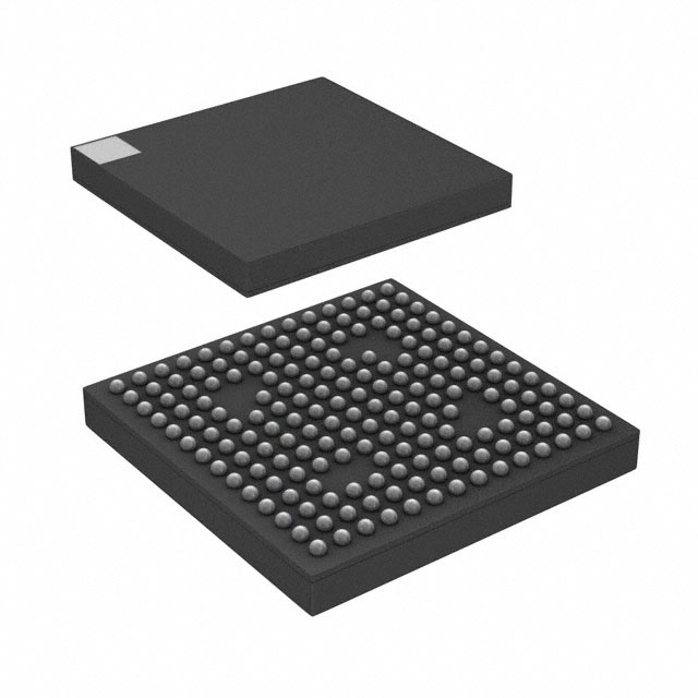
- Part No.:
- ADSP-BF705KBCZ-3
- Manufacturer:
- Analog Devices Inc.
- Category:
- DSP (Digital Signal Processors)
- Package:
- 184-LFBGA, CSPBGA
- Datasheet:
-
 ADSP-BF705KBCZ-3.pdf
- Description:
- IC DSP LP 512KB L2SR 184BGA
- Quantity:
- Payment:

- Shipping:

Inventory:3,559
Please send an inquiry. Send us your inquiry, and we will respond immediately.
Product details
Overview
ADSP-BF705KBCZ-3 from Analog Devices is a Blackfin+ embedded processor IC delivering 400 MHz peak performance with dual 16-bit or single 32-bit MAC per cycle, 136 kB parity-protected L1 SRAM (64 kB instruction + 64 kB data + 8 kB scratchpad), and AEC-Q100 qualification for automotive control systems requiring deterministic real-time signal processing.
For engineers reviewing the ADSP-BF705KBCZ-3 datasheet, ADSP-BF705KBCZ-3 pinout, ADSP-BF705KBCZ-3 application, or ADSP-BF705KBCZ-3 equivalent, key selection considerations include its 184-ball CSP_BGA package, integrated crypto accelerators, dual CAN 2.0B interfaces, USB 2.0 HS OTG, and L2 SRAM variants up to 1 MB with ECC protection.
Technical Context
The ADSP-BF705KBCZ-3 implements a modified Harvard architecture with separate 64 kB L1 instruction and 64 kB L1 data SRAM blocks-both multi-parity-bit protected-and an 8 kB L1 scratchpad. Its Blackfin+ core integrates two 16-bit multipliers, one 32-bit multiplier, dual 40-bit ALUs, and a 72-bit ALU supporting simultaneous 16-bit operations on register pairs.
It features a hierarchical memory system: L2 SRAM (512 kB) with ECC, 512 kB L2 ROM, and optional L3 interface (CSP_BGA only) for DDR2/LPDDR at up to 200 MHz. Peripherals include two CAN controllers, two UARTs, two SPORTs, PPI, MSI (SD/SDIO), USB 2.0 HS OTG, and hardware crypto engines for secure boot and memDMA encryption.
Key Specifications
| Parameter | Value and Actual Design Meaning |
|---|---|
| Core Architecture | Blackfin+ 32-bit RISC/DSP hybrid with instruction set compatibility to prior Blackfin processors |
| Max Operating Frequency | 400 MHz - enables real-time audio/video analytics and motor control loop execution within sub-μs latency |
| L1 Memory | 136 kB total: 64 kB instruction SRAM, 64 kB data SRAM, 8 kB scratchpad - all with multi-parity-bit protection for safety-critical operation |
| L2 Memory | 512 kB SRAM with ECC protection - supports robust firmware storage and runtime data buffers without external DRAM dependency |
| Package | 184-ball CSP_BGA, 12 mm × 12 mm × 0.8 mm pitch - RoHS-compliant, optimized for automotive thermal and vibration environments |
| Automotive Qualification | AEC-Q100 Grade 3 (−40°C to +125°C) - validated for engine control units, ADAS sensor fusion, and infotainment subsystems |
| Security Features | Crypto hardware accelerators (AES, SHA, RSA), OTP memory (1 kB), fast secure boot - enables IP protection and authenticated firmware updates |
Pinout & Package
ADSP-BF705KBCZ-3 uses a 184-ball CSP_BGA package (12 mm × 12 mm, 0.8 mm pitch), RoHS compliant, with ball assignments defined in Analog Devices' ADSP-BF70x datasheet Rev. D, pages 105–107. The package supports full peripheral access including dual CAN, USB 2.0 HS OTG, DDR2/LPDDR via L3 interface, and 47 GPIOs with flexible multiplexing.
| Pin/Terminal | Circuit Role | Design Meaning |
|---|---|---|
| VDD_INT | Core power supply | 1.0 V ±3% supply for Blackfin+ core - requires low-noise regulation due to high-frequency switching sensitivity |
| VDD_EXT | I/O and peripheral power | 3.3 V ±5% supply for GPIO, CAN, UART, USB PHY - supports mixed-voltage interfacing with external sensors and transceivers |
| CLKIN | External clock input | Accepts 1–50 MHz crystal or oscillator input - feeds PLL for generating 400 MHz SYSCLK and peripheral clocks |
| RESET | Active-low reset input | Synchronous deassertion required after power stabilization - initiates secure boot sequence from L2 ROM or external memory |
| CAN0_TX / CAN0_RX | Controller Area Network channel 0 | Differential signaling pair compliant with ISO 11898-2 - supports 1 Mbps automotive bus communication with built-in protocol handling |
| USB_DP / USB_DM | USB 2.0 High-Speed differential pair | Integrated PHY supports host/device/OTG modes - eliminates need for external transceiver in telematics and diagnostic applications |
Key Features
| Feature | Design Value |
|---|---|
| Dual CAN 2.0B controllers | Enables concurrent communication on two isolated automotive buses - supports message filtering, FIFO buffering, and error confinement for ECU domain controllers |
| Hardware crypto acceleration | Offloads AES-128/256, SHA-256, and RSA operations from CPU - reduces secure boot time to <100 ms and enables real-time encrypted data streaming |
| 8-channel general-purpose timers | Supports PWM generation, input capture, quadrature decoding, and watchdog functions - configurable for motor phase timing and encoder position tracking |
| Static Memory Controller (SMC) | Manages up to two external parallel devices (NOR flash, SRAM, FPGA) with programmable timing - simplifies BOM by eliminating glue logic in industrial HMI designs |
| Multi-protocol serial interfaces | 2× SPORT (synchronous serial), 2× UART, 1× PPI, 4-bit/8-bit MSI (SD/SDIO), Quad/Dual SPI - enables direct connection to ADCs, displays, cameras, and memory cards without bridge ICs |
Applications
| Automotive Engine Control Unit (ECU) | Industrial Motor Drive Controller |
|---|---|
Use Scenario: Real-time combustion timing, fuel injection pulse width modulation, and OBD-II diagnostics in gasoline/diesel powertrains. IC Role / Device Role / Timing Role: Primary compute engine executing closed-loop PID control at 10 kHz, managing CAN FD-capable communication with sensors and actuators. Use Value: Deterministic 400 MHz Blackfin+ core with 136 kB protected L1 SRAM ensures sub-microsecond interrupt latency and fault-tolerant execution under ASIL-B conditions. |
Use Scenario: Field-oriented control (FOC) of 3-phase BLDC/PMSM motors in HVAC compressors and factory automation drives. IC Role / Device Role / Timing Role: Real-time DSP engine performing Park/Clarke transforms, space-vector PWM generation, and current loop regulation at 20 kHz switching frequency. Use Value: Dual 16-bit MAC per cycle and dedicated video ALUs accelerate motor control math while L2 ECC SRAM prevents data corruption during EMI-heavy operation. |
| Medical Ultrasound Beamformer | Smart Energy Meter with Secure Firmware |
Use Scenario: Digital beamforming and RF echo processing in portable ultrasound systems with multi-channel analog front-end. IC Role / Device Role / Timing Role: Signal co-processor handling time-aligned FIR filtering, envelope detection, and log compression before display rendering. Use Value: 16-bit complex MAC support and 2D DMA enable synchronized processing across 64+ channels with zero buffer copy overhead. |
Use Scenario: ANSI C12.22-compliant smart meter with tamper detection, encrypted firmware updates, and dual tariff billing logic. IC Role / Device Role / Timing Role: Secure host controller managing metrology SoC communication, secure boot validation, and TLS stack execution. Use Value: On-chip crypto accelerators and 1 kB OTP memory provide hardware-rooted trust for firmware signature verification and AES-GCM encrypted OTA updates. |
Equivalent & Alternatives
The following parts are listed as comparable options for similar embedded signal processing applications.
| Alternative Part | Technical Difference | Application Difference | Selection Advice |
|---|---|---|---|
| ADSP-BF706KBCZ-3 | 1 MB L2 SRAM (vs. 512 kB), DDR2/LPDDR L3 interface enabled, same 184-ball CSP_BGA package | Required for applications needing >512 kB off-core code/data storage without external DRAM | Select when larger L2 footprint is needed for complex algorithm libraries or multi-threaded RTOS workloads |
| NXP i.MX RT1052CVL5B | ARM Cortex-M7 @ 600 MHz, 512 kB on-chip SRAM, no integrated crypto accelerators, different peripheral set (no CAN 2.0B, no SPORT) | Better suited for Linux-capable edge AI inference or GUI-rich HMI where ARM ecosystem tooling is preferred | Choose for higher integer throughput and CMSIS-NN compatibility; avoid if legacy Blackfin codebase or CAN/audio co-processing is required |
Compared with ADSP-BF705KBCZ-3, ADSP-BF706KBCZ-3 offers double L2 capacity for larger firmware images, while NXP i.MX RT1052CVL5B trades deterministic DSP capability for raw Cortex-M7 integer performance and broader software support-making ADSP-BF705KBCZ-3 optimal for cost-sensitive, safety-aware signal processing where Blackfin instruction efficiency and peripheral integration matter most.
Availability
ADSP-BF705KBCZ-3 is available at Aetrix Electronics and suitable for automotive ECU development, industrial motor control systems, medical imaging subsystems, and secure smart metering applications requiring stable component supply and long-term lifecycle assurance.
Supply support for ADSP-BF705KBCZ-3 includes scheduled delivery planning, volume procurement assistance, BOM continuity management, traceable sourcing, and lifecycle availability coordination for OEM customers, industrial embedded developers, connected-device designers, and electronics production programs.
Manufacturer
Analog Devices, Inc. is a global leader in high-performance analog, mixed-signal, and digital signal processing technology, headquartered in Norwood, MA, with design centers and manufacturing facilities worldwide.
The ADSP-BF70x product line was engineered specifically for cost-sensitive, power-constrained embedded applications demanding both real-time DSP performance and MCU programmability-targeting automotive, industrial, and medical markets where functional safety and security are foundational.
FAQ
What is the maximum operating temperature range for ADSP-BF705KBCZ-3?
The ADSP-BF705KBCZ-3 is AEC-Q100 qualified for Grade 3 operation, supporting junction temperatures from −40°C to +125°C. This rating is validated across the full 400 MHz operating frequency and applies to all I/O banks and internal logic. Thermal derating is not required within this range, making ADSP-BF705KBCZ-3 suitable for under-hood automotive modules and industrial enclosures without active cooling.
Does ADSP-BF705KBCZ-3 support secure boot from external flash?
Yes, ADSP-BF705KBCZ-3 supports secure boot from external SPI flash via its Quad SPI interface using hardware-accelerated AES-256 decryption. The boot ROM validates signed firmware images stored in external memory, then loads decrypted code into protected L1 SRAM. This process leverages the on-chip crypto engine and 1 kB OTP memory storing root keys-ensuring ADSP-BF705KBCZ-3 meets IEC 62443-3-3 SL2 requirements for secure firmware update.
How many CAN interfaces does ADSP-BF705KBCZ-3 integrate, and what protocol versions are supported?
ADSP-BF705KBCZ-3 integrates two independent CAN 2.0B controllers compliant with ISO 11898-1. Each supports standard (11-bit) and extended (29-bit) identifier formats, bit rates up to 1 Mbps, and full mailbox-based message buffering with hardware acceptance filtering. Neither controller supports CAN FD; for CAN FD applications, ADSP-BF705KBCZ-3 must be paired with an external transceiver and protocol handler.
Is external DDR memory required to use ADSP-BF705KBCZ-3?
No, ADSP-BF705KBCZ-3 operates fully autonomously using its on-chip memories: 136 kB protected L1 SRAM and 512 kB ECC-protected L2 SRAM. External DDR2 or LPDDR is optional and accessed only via the L3 interface (enabled in CSP_BGA packages). Most real-time control and signal processing applications run entirely from internal memory-eliminating DDR complexity, cost, and power consumption unless large frame buffers or OS support are needed.
What development tools are officially supported for ADSP-BF705KBCZ-3?
Analog Devices provides full toolchain support for ADSP-BF705KBCZ-3 via CrossCore Embedded Studio (CCES), including C/C++ compiler, assembler, linker, JTAG debugger, and RTOS-agnostic libraries. Hardware debugging uses ICE-1000/2000 emulators with SWD/JTAG. Reference schematics, IBIS models, and validated PCB layout guidelines are published in the ADSP-BF70x Hardware Reference Manual (Rev. D), ensuring reliable bring-up of ADSP-BF705KBCZ-3 in production designs.
ADSP-BF705KBCZ-3 Specifications
- Product attributes
- Attribute value
- Manufacturer:
- Analog Devices Inc.
- Series:
- Blackfin®
- Package/Case:
- 184-LFBGA, CSPBGA
- Packaging:
- Tray
- Product Status:
- Active
- Type:
- Blackfin+
- Interface:
- CAN, DSPI, EBI/EMI, I2C, PPI, QSPI, SD/SDIO, SPI, SPORT, UART/USART, USB OTG
- Clock Rate:
- 300MHz
- Non-Volatile Memory:
- ROM (512kB)
- On-Chip RAM:
- 512kB
- Voltage - I/O:
- 1.8V, 3.3V
- Voltage - Core:
- 1.10V
- Operating Temperature:
- 0°C ~ 70°C (TA)
- Grade:
- -
- Qualification:
- -
- Mounting Type:
- Surface Mount
- Supplier Device Package:
- 184-CSPBGA (12x12)
ADSP-BF705KBCZ-3 FAQ
1.How can I place an order for ADSP-BF705KBCZ-3 through Aetrix?
Please submit a Request for Quotation (RFQ) for ADSP-BF705KBCZ-3 on Aetrix. Our sales agent will provide a competitive quotation and guide you through the order confirmation once you accept the terms.
2.Are the price and stock information for ADSP-BF705KBCZ-3 reliable?
The price and inventory of ADSP-BF705KBCZ-3 are updated periodically and may fluctuate due to market conditions. Stock and pricing data are typically refreshed every 24 hours. Quotation validity for ADSP-BF705KBCZ-3 is usually 5 days.
3.What payment methods are accepted for ADSP-BF705KBCZ-3?
We accept Wire Transfer, PayPal, Credit Card, Western Union, MoneyGram, and Escrow for ADSP-BF705KBCZ-3 transactions.
Note: Certain payment methods may incur a processing fee.
4.How is shipping managed for ADSP-BF705KBCZ-3?
ADSP-BF705KBCZ-3 orders can be shipped via leading logistics carriers, including DHL, UPS, FedEx, TNT, or Registered Mail.
Once your ADSP-BF705KBCZ-3 order is processed, you will receive an email with the shipment details and tracking number.
Note: Tracking information may take up to 24 hours to appear. Express delivery typically takes 3–5 business days.
5.How can I obtain technical support or documentation for ADSP-BF705KBCZ-3?
For technical support, including ADSP-BF705KBCZ-3 datasheets, pinout diagrams, or application guidance, please contact our engineering support team. They can provide detailed documentation and assistance for your ADSP-BF705KBCZ-3 requirements.
6.How does Aetrix verify that ADSP-BF705KBCZ-3 is sourced from the original manufacturer or authorized distributors?
All ADSP-BF705KBCZ-3 products on Aetrix are procured from qualified distributors and authorized channels. Our dedicated quality assurance team conducts strict verification, including traceability checks and, if necessary, third-party testing. This ensures that ADSP-BF705KBCZ-3 meets industry standards.
7.What is the process for return or replacement of ADSP-BF705KBCZ-3?
All ADSP-BF705KBCZ-3 units undergo pre-shipment inspection (PSI). If there is an issue with ADSP-BF705KBCZ-3, returns or replacements are accepted under the following conditions:
1.Quantity discrepancies, incorrect items, or visible external defects (such as breakage or corrosion), acknowledged by Aetrix.
2.The issue is reported within 90 days of delivery.
3.The ADSP-BF705KBCZ-3 part is unused and in its original packaging.
Return procedure for ADSP-BF705KBCZ-3:
1.Submit a request within 90 days.
2.Obtain a Return Material Authorization (RMA) from Aetrix.
ADSP-BF705KBCZ-3 Tags
-
TMS320C5535AZAY10
Texas Instruments
-
TMS320VC5501PGF300
Texas Instruments
-
ADSP-BF592KCPZ
Analog Devices Inc.
-
ADAU1463WBCPZ150
Analog Devices Inc.

-
TMS320VC5402PGE100
Texas Instruments

-
ADAU1701JSTZ-RL
Analog Devices Inc.
-
ADAU1701JSTZ
Analog Devices Inc.
-
TMS320VC5502PGF300
Texas Instruments
-
ADAU1462WBCPZ300RL
Analog Devices Inc.
-
ADAU1452KCPZRL
Analog Devices Inc.
-
ADAU1452WBCPZ-RL
Analog Devices Inc.
-
TMS320C6747DZKB3
Texas Instruments
Tech Hub

A practical engineering guide to 3.3V and 5V logic compatibility, input thresholds, resistor dividers, translator ICs, MOSFET level shifting, I2C pull-ups, timing limits and power-sequencing risks.

The 74HC595 uses push-pull logic outputs, while the TPIC6B595 uses 50 V open-drain DMOS sinks for higher-power loads. This guide compares timing, current limits, 3.3 V interfacing, load wiring, thermal…

The 74HC595 converts serial data into eight stable parallel outputs. This guide covers pin functions, shift and storage timing, OE and MR behavior, drive-current limits, cascading, voltage compatibilit…

A technical comparison of level-sensitive latches and edge-triggered flip-flops, covering timing windows, setup and hold limits, master–slave operation, time borrowing, race-through, HDL inference and…

A D latch stores one bit while Enable controls when data can pass. This reference covers gate-level operation, truth tables, transparency, setup and hold timing, LE versus OE, common ICs and practical …

An SR latch stores one bit through cross-coupled feedback. This engineering reference covers NOR and NAND implementations, truth tables, forbidden-state recovery, gated operation, switch debouncing, fa…

Latch circuits retain one bit through feedback. This technical reference covers SR and D latches, truth tables, transparency, timing limits, latch-versus-flip-flop behavior, applications and common log…

An engineering guide to LED driver operation, constant-current and constant-voltage outputs, linear and switching topologies, dimming, IC selection, calculations, replacement compatibility, and fault c…

Operational amplifier guide covering op amp basics, feedback, ideal vs real op amps, common configurations, buffer circuits, offset, bias current, gain-bandwidth, slew rate, rail-to-rail limits and sel…

Jumper cables guide covering safe connection order, red and black clamp placement, final ground connection, cable gauge, length, clamp quality, copper vs CCA cables, jump starter comparison and battery…


