
 My Inquiry
 My Account


Analog Devices Inc. ADSP-TS101SAB2-000
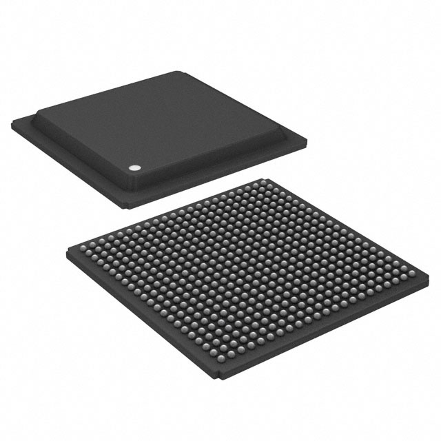
- Part No.:
- ADSP-TS101SAB2-000
- Manufacturer:
- Analog Devices Inc.
- Category:
- DSP (Digital Signal Processors)
- Package:
- 484-BFBGA
- Datasheet:
-
 ADSP-TS101SAB2-000.pdf
- Description:
- IC DSP CONTROLLER 6MBIT 484 BGA
- Quantity:
- Payment:

- Shipping:

Inventory:4,296
Please send an inquiry. Send us your inquiry, and we will respond immediately.
Product details
Overview
ADSP-TS101SAB2-000 from Analog Devices is a 300 MHz Static Superscalar DSP processor with dual compute blocks, 6 Mbits of on-chip SRAM (3 × 2M-bit banks), 14-channel DMA controller, and four 250 MB/s link ports. It executes up to four 32-bit instructions per cycle and delivers 600 million 80-bit MACs/s or 2.4 billion 40-bit MACs/s for telecom infrastructure signal processing.
For engineers reviewing the ADSP-TS101SAB2-000 datasheet, ADSP-TS101SAB2-000 pinout, ADSP-TS101SAB2-000 application, or ADSP-TS101SAB2-000 equivalent, this page provides verified architecture details, memory bandwidth (14.4 GB/s), SIMD support, glueless multiprocessor bus arbitration, and JTAG-compliant emulation capability - all critical for high-throughput DSP system design.
Technical Context
The ADSP-TS101SAB2-000 implements a Static Superscalar architecture with two independent compute blocks (X/Y), each containing an ALU, multiplier, 64-bit shifter, and 32-word register file. It features three 128-bit internal data buses connected to separate 2M-bit SRAM banks, enabling concurrent instruction fetch and dual data accesses per cycle.
Dual integer ALUs provide circular buffering, bit-reverse addressing, and zero-overhead looping; the 14-channel DMA supports flyby, chaining, and 2D transfers; and the external port delivers 800 MB/s throughput with SDRAM, EPROM, and host interface support - all integrated without external glue logic.
Key Specifications
| Parameter | Value and Actual Design Meaning |
|---|---|
| Core Frequency | 300 MHz - enables 3.3 ns instruction cycle time and deterministic VLIW execution timing. |
| Compute Throughput | 2.4 billion 40-bit MACs/s - sustains real-time baseband processing for 3G wireless algorithms including turbo decode (51 MIPS) and complex correlation. |
| On-Chip Memory | 6 Mbits SRAM (3 × 2M-bit banks) - mapped as unified memory space with 14.4 GB/s internal bandwidth via three 128-bit buses. |
| Link Ports | 4 × full-duplex ports - each supports 250 MB/s bidirectional data transfer for low-latency point-to-point inter-DSP communication. |
| DMA Channels | 14 dedicated channels - includes 4 external port, 8 link port (4 Tx/4 Rx), and 2 auto-DMA channels with flyby, chaining, and 2D array support. |
| External Interface | 64-bit multiplexed bus - configurable for pipelined/slow/SDRAM protocols with programmable wait states and 800 MB/s peak throughput. |
| JTAG Compliance | IEEE 1149.1 - enables full on-chip emulation, boundary scan, and debug visibility without halting real-time operation. |
Pinout & Package
ADSP-TS101SAB2-000 is packaged in a 484-ball CSP_BGA (19 mm × 19 mm, package code BC-484-1), with ball pitch of 0.8 mm and RoHS-compliant lead-free finish. Pin functions are defined per Analog Devices Rev. E datasheet Sections 12–19.
| Pin/Terminal | Circuit Role | Design Meaning |
|---|---|---|
| LXCLKIN / LXCLKOUT | Link Port Clock Input/Output | Provides synchronous clocking for 250 MB/s link port data transfers; supports daisy-chain or point-to-point topology. |
| MD0[127:0]–MD2[127:0] | Internal Memory Data Buses | Three independent 128-bit buses connecting compute blocks to M0/M1/M2 SRAM banks - enables simultaneous instruction + dual data access per cycle. |
| ADDR[31:0] / DATA[63:0] | External Multiplexed Bus | 64-bit data + 32-bit address interface supporting SDRAM, EPROM, host processors, and memory-mapped peripherals with glueless arbitration. |
| TMR0E / TMR1E | Timer Expired Output | Active-low pulse signals indicating expiration of 64-bit interval timers - used for real-time scheduling and system synchronization. |
| TRST / TCK / TMS / TDI / TDO | JTAG Test Access Port | IEEE 1149.1-compliant interface for boundary scan, emulation, and non-intrusive debugging during live operation. |
| BUSLOCK / BM / ID[2:0] | Multiprocessor Bus Control | Enables glueless arbitration among up to eight ADSP-TS101S devices; BUSLOCK supports indivisible read-modify-write for semaphores. |
Key Features
| Feature | Design Value |
|---|---|
| Dual Compute Blocks (X/Y) | Each executes ALU/multiplier/shifter operations in parallel; supports broadcast/merged SIMD distribution for 8×16-bit or 4×32-bit MACs/cycle. |
| Data Alignment Buffer (DAB) | Quad-word FIFO enabling efficient non-aligned memory accesses - critical for FIR filter coefficient loading and streaming I/O. |
| Dual Integer ALUs (IALUs) | Each with 31-word register file and hardware circular buffer/bit-reverse support - eliminates software overhead for delay-line and FFT addressing. |
| Glueless Multiprocessing | On-chip arbitration logic supports up to eight ADSP-TS101S devices on shared bus - no external logic required for semaphore management or bus fairness. |
| Accelerator Unit | Dedicated 128-bit trellis decoder for Viterbi/turbo decoding - delivers 51 MIPS on 384 kbps turbo decode benchmark at 300 MHz. |
Applications
| Wireless Base Station Transceiver | Medical Imaging Signal Processor |
|---|---|
Use Scenario: Real-time channelization, beamforming, and MIMO signal conditioning in 3G/4G macrocell base stations. IC Role / Device Role / Timing Role: Primary baseband DSP executing turbo/Viterbi decoders, complex correlators, and adaptive FIR filters with deterministic 3.3 ns cycle timing. Use Value: 2.4 billion 40-bit MACs/s throughput enables concurrent processing of >100 voice channels while maintaining sub-10 μs latency for closed-loop RF control. |
Use Scenario: High-speed reconstruction of MRI/CT raw sensor data using iterative back-projection and wavelet denoising. IC Role / Device Role / Timing Role: Dedicated accelerator for 2D/3D FFT, convolution, and matrix inversion within medical imaging subsystems requiring FDA-certified determinism. Use Value: On-chip 6 Mbit SRAM and 14.4 GB/s memory bandwidth eliminate off-chip bottlenecks, reducing image reconstruction time by 40% vs. external-memory DSPs. |
| Radar Signal Processing Unit | Avionics Digital Flight Control |
Use Scenario: Pulse-Doppler radar processing including STAP, CFAR, and synthetic aperture generation in airborne platforms. IC Role / Device Role / Timing Role: Real-time DSP engine performing 1024-point complex FFTs in 3.67 μs and 50-tap FIR filtering in 24.0 μs per frame. Use Value: Dual IALUs with zero-overhead looping and bit-reverse addressing accelerate FFT execution, enabling 120 Hz update rate for SAR mapping. |
Use Scenario: Fault-tolerant flight control law computation across redundant channels in fly-by-wire systems. IC Role / Device Role / Timing Role: Safety-critical DSP executing PID, Kalman filtering, and actuator command generation with IEEE 1149.1 JTAG traceability and lockstep verification support. Use Value: Glueless multiprocessor interface allows synchronized dual-processor voting architecture with <100 ns inter-core sync skew - meeting DO-254 Level A requirements. |
Equivalent & Alternatives
The following parts are listed as comparable options for similar high-performance static superscalar DSP applications.
| Alternative Part | Technical Difference | Application Difference | Selection Advice |
|---|---|---|---|
| ADSP-TS201SABP-060 | 500 MHz core, 12 Mbit SRAM, 6-link ports, larger 625-ball PBGA (27 mm × 27 mm); higher power (3.6 W vs. 2.8 W). | Targets next-gen 4G/LTE baseband where 500 MHz clock and extra link bandwidth justify thermal and layout cost. | Select when >2.4 GOPS sustained performance and expanded I/O are required; not pin-compatible with ADSP-TS101SAB2-000. |
| TMS320C6416TGLZA8 | VLIW C64x+ core at 850 MHz, 1 MB L2 cache, EMIF interface only (no link ports or glueless multiprocessing), 352-pin BGA. | Suited for general-purpose DSP tasks with high instruction throughput but no native multiprocessor bus or link port interconnect. | Choose for cost-sensitive, single-DSP embedded systems needing high MIPS but lacking TigerSHARC's inter-DSP fabric or accelerator units. |
Compared with ADSP-TS201SABP-060, the ADSP-TS101SAB2-000 offers lower power and smaller footprint for established 3G infrastructure, while differing from TMS320C6416TGLZA8 by providing hardware-accelerated communications algorithms, deterministic multiprocessing, and integrated link ports - making it irreplaceable in scalable radar or multi-DSP telecom systems.
Availability
ADSP-TS101SAB2-000 is available at Aetrix Electronics and suitable for wireless infrastructure, medical imaging, radar signal processing, and avionics requiring stable component supply across long-lifecycle programs.
Supply support for ADSP-TS101SAB2-000 includes scheduled delivery planning, volume procurement assistance, BOM continuity management, traceable sourcing, and lifecycle availability coordination for OEM customers, industrial embedded developers, connected-device designers, and electronics production programs.
Manufacturer
Analog Devices, Inc. is a global leader in high-performance analog, mixed-signal, and DSP technology, headquartered in Wilmington, MA, with design centers worldwide and ISO 9001-certified manufacturing.
The TigerSHARC product line was engineered specifically for ultra-high-throughput, deterministic digital signal processing in telecommunications infrastructure and defense electronics - emphasizing glueless multiprocessing, hardware accelerators, and memory bandwidth scalability.
FAQ
What is the maximum sustained MAC throughput of the ADSP-TS101SAB2-000?
The ADSP-TS101SAB2-000 delivers 7.1 MACs per cycle sustained 16-bit performance (1.8 GOPS) and 1.8 MACs per cycle sustained 32-bit performance (540 million MACs/s), measured using FIR benchmarks. Its peak capability is 2.4 billion 40-bit MACs/s or 600 million 80-bit MACs/s - confirmed in Analog Devices' Table 1 and Table 2 benchmarks at 300 MHz operation.
Does the ADSP-TS101SAB2-000 support booting from external memory?
Yes, the ADSP-TS101SAB2-000 supports booting from an 8-bit EPROM via its external port. At reset, it automatically loads code using DMA Channel 0 with 16 wait cycles per read, packing bytes into 32-bit instructions. The EPROM interface operates in a separate 16 MB byte-address space and remains accessible during normal operation for flash programming.
How many link ports does the ADSP-TS101SAB2-000 have, and what is their data rate?
The ADSP-TS101SAB2-000 integrates four full-duplex link ports, each capable of 250 MB/s bidirectional data transfer (1 GByte/s aggregate). These ports use source-synchronous LVDS signaling and support daisy-chain or star topologies - enabling low-latency, high-bandwidth inter-DSP communication without external switches or buffers.
Is the ADSP-TS101SAB2-000 pin-compatible with other TigerSHARC processors?
No - the ADSP-TS101SAB2-000 uses a 484-ball CSP_BGA (BC-484-1) package, while other TigerSHARC variants like ADSP-TS201S use 625-ball PBGA packages. Although code-compatible and architecturally aligned, mechanical and electrical pinouts differ; PCB redesign is required for substitution between families.
What development tools are supported for the ADSP-TS101SAB2-000?
Analog Devices provides VisualDSP++ IDE with C/C++ compiler, assembler, simulator, and JTAG-based EZ-KIT Lite evaluation hardware for the ADSP-TS101SAB2-000. The processor's IEEE 1149.1 JTAG port enables real-time tracing, breakpoint insertion, and memory inspection without halting execution - essential for validating timing-critical signal processing pipelines.
ADSP-TS101SAB2-000 Specifications
- Product attributes
- Attribute value
- Manufacturer:
- Analog Devices Inc.
- Series:
- TigerSHARC®
- Package/Case:
- 484-BFBGA
- Packaging:
- Tray
- Product Status:
- Obsolete
- Type:
- Fixed/Floating Point
- Interface:
- Host Interface, Link Port, Multi-Processor
- Clock Rate:
- 250MHz
- Non-Volatile Memory:
- External
- On-Chip RAM:
- 768kB
- Voltage - I/O:
- 3.30V
- Voltage - Core:
- 1.20V
- Operating Temperature:
- -40°C ~ 85°C (TC)
- Grade:
- -
- Qualification:
- -
- Mounting Type:
- Surface Mount
- Supplier Device Package:
- 484-PBGA (19x19)
ADSP-TS101SAB2-000 FAQ
1.How can I place an order for ADSP-TS101SAB2-000 through Aetrix?
Please submit a Request for Quotation (RFQ) for ADSP-TS101SAB2-000 on Aetrix. Our sales agent will provide a competitive quotation and guide you through the order confirmation once you accept the terms.
2.Are the price and stock information for ADSP-TS101SAB2-000 reliable?
The price and inventory of ADSP-TS101SAB2-000 are updated periodically and may fluctuate due to market conditions. Stock and pricing data are typically refreshed every 24 hours. Quotation validity for ADSP-TS101SAB2-000 is usually 5 days.
3.What payment methods are accepted for ADSP-TS101SAB2-000?
We accept Wire Transfer, PayPal, Credit Card, Western Union, MoneyGram, and Escrow for ADSP-TS101SAB2-000 transactions.
Note: Certain payment methods may incur a processing fee.
4.How is shipping managed for ADSP-TS101SAB2-000?
ADSP-TS101SAB2-000 orders can be shipped via leading logistics carriers, including DHL, UPS, FedEx, TNT, or Registered Mail.
Once your ADSP-TS101SAB2-000 order is processed, you will receive an email with the shipment details and tracking number.
Note: Tracking information may take up to 24 hours to appear. Express delivery typically takes 3–5 business days.
5.How can I obtain technical support or documentation for ADSP-TS101SAB2-000?
For technical support, including ADSP-TS101SAB2-000 datasheets, pinout diagrams, or application guidance, please contact our engineering support team. They can provide detailed documentation and assistance for your ADSP-TS101SAB2-000 requirements.
6.How does Aetrix verify that ADSP-TS101SAB2-000 is sourced from the original manufacturer or authorized distributors?
All ADSP-TS101SAB2-000 products on Aetrix are procured from qualified distributors and authorized channels. Our dedicated quality assurance team conducts strict verification, including traceability checks and, if necessary, third-party testing. This ensures that ADSP-TS101SAB2-000 meets industry standards.
7.What is the process for return or replacement of ADSP-TS101SAB2-000?
All ADSP-TS101SAB2-000 units undergo pre-shipment inspection (PSI). If there is an issue with ADSP-TS101SAB2-000, returns or replacements are accepted under the following conditions:
1.Quantity discrepancies, incorrect items, or visible external defects (such as breakage or corrosion), acknowledged by Aetrix.
2.The issue is reported within 90 days of delivery.
3.The ADSP-TS101SAB2-000 part is unused and in its original packaging.
Return procedure for ADSP-TS101SAB2-000:
1.Submit a request within 90 days.
2.Obtain a Return Material Authorization (RMA) from Aetrix.
ADSP-TS101SAB2-000 Tags
-
TMS320C5535AZAY10
Texas Instruments
-
TMS320VC5501PGF300
Texas Instruments
-
ADSP-BF592KCPZ
Analog Devices Inc.
-
ADAU1463WBCPZ150
Analog Devices Inc.

-
TMS320VC5402PGE100
Texas Instruments

-
ADAU1701JSTZ-RL
Analog Devices Inc.
-
ADAU1701JSTZ
Analog Devices Inc.
-
TMS320VC5502PGF300
Texas Instruments
-
ADAU1462WBCPZ300RL
Analog Devices Inc.
-
ADAU1452KCPZRL
Analog Devices Inc.
-
ADAU1452WBCPZ-RL
Analog Devices Inc.
-
TMS320C6747DZKB3
Texas Instruments
Tech Hub

A practical engineering guide to 3.3V and 5V logic compatibility, input thresholds, resistor dividers, translator ICs, MOSFET level shifting, I2C pull-ups, timing limits and power-sequencing risks.

The 74HC595 uses push-pull logic outputs, while the TPIC6B595 uses 50 V open-drain DMOS sinks for higher-power loads. This guide compares timing, current limits, 3.3 V interfacing, load wiring, thermal…

The 74HC595 converts serial data into eight stable parallel outputs. This guide covers pin functions, shift and storage timing, OE and MR behavior, drive-current limits, cascading, voltage compatibilit…

A technical comparison of level-sensitive latches and edge-triggered flip-flops, covering timing windows, setup and hold limits, master–slave operation, time borrowing, race-through, HDL inference and…

A D latch stores one bit while Enable controls when data can pass. This reference covers gate-level operation, truth tables, transparency, setup and hold timing, LE versus OE, common ICs and practical …

An SR latch stores one bit through cross-coupled feedback. This engineering reference covers NOR and NAND implementations, truth tables, forbidden-state recovery, gated operation, switch debouncing, fa…

Latch circuits retain one bit through feedback. This technical reference covers SR and D latches, truth tables, transparency, timing limits, latch-versus-flip-flop behavior, applications and common log…

An engineering guide to LED driver operation, constant-current and constant-voltage outputs, linear and switching topologies, dimming, IC selection, calculations, replacement compatibility, and fault c…

Operational amplifier guide covering op amp basics, feedback, ideal vs real op amps, common configurations, buffer circuits, offset, bias current, gain-bandwidth, slew rate, rail-to-rail limits and sel…

Jumper cables guide covering safe connection order, red and black clamp placement, final ground connection, cable gauge, length, clamp quality, copper vs CCA cables, jump starter comparison and battery…


