
 My Inquiry
 My Account


Analog Devices Inc. ADUM5403WCRWZ-1
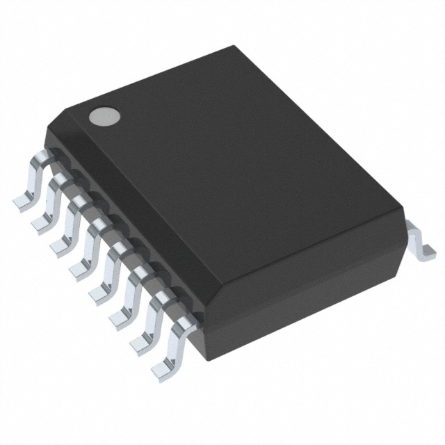
- Part No.:
- ADUM5403WCRWZ-1
- Manufacturer:
- Analog Devices Inc.
- Category:
- Digital Isolators
- Package:
- 16-SOIC (0.295", 7.50mm Width)
- Datasheet:
-
 ADUM5403WCRWZ-1.pdf
- Description:
- DGTL ISO 2500VRMS 4CH GP 16SOIC
- Quantity:
- Payment:

- Shipping:

Inventory:3,700
Please send an inquiry. Send us your inquiry, and we will respond immediately.
Product details
Overview
ADUM5403WCRWZ-1 from Analog Devices is a quad-channel digital isolator with integrated isoPower® dc-to-dc converter, delivering regulated 3.3 V isolated output up to 89 mA (5 V input / 3.3 V output mode), supporting 25 Mbps NRZ data rates, and qualified for automotive applications with 105°C operation and 7.6 mm creepage in 16-lead SOIC package. It enables compact battery management and motor control interfaces where galvanic isolation and local power are both required.
For engineers reviewing the ADUM5403WCRWZ-1 datasheet, ADUM5403WCRWZ-1 pinout, ADUM5403WCRWZ-1 application, or ADUM5403WCRWZ-1 equivalent, key selection criteria include its 25 Mbps channel speed, 3.3 V isolated supply capability under 5 V primary input, 25 kV/µs common-mode transient immunity, reinforced insulation rating (VIORM = 565 V peak), and automotive qualification per AEC-Q100.
Technical Context
The ADUM5403WCRWZ-1 implements iCoupler® chip-scale transformer technology for both signal isolation and magnetic power transfer, eliminating external isolated DC/DC converters. Its internal PWM-controlled oscillator operates at 625 kHz with 180 MHz switching frequency, enabling up to 500 mW total isolated power (derated to 297 mW at 3.3 V output under 5 V input).
It features codirectional channel matching of ≤6 ns skew and opposing-directional skew ≤15 ns, with propagation delay ≤60 ns and pulse width distortion ≤6 ns across all four channels. The device includes undervoltage lockout (2.4 V–2.7 V thresholds) on both VDD1 and VISO rails and supports dual-supply configurations (5 V/5 V, 5 V/3.3 V, or 3.3 V/3.3 V).
Key Specifications
| Parameter | Value and Actual Design Meaning |
|---|---|
| Data Rate | 25 Mbps NRZ - supports high-speed CAN FD, SPI, and RS-485 interface isolation without timing bottlenecks |
| Isolated Output Voltage | 3.3 V (regulated) - powers downstream isolated logic (e.g., gate drivers, ADCs) directly from primary-side 5 V rail |
| Max Isolated Output Current | 89 mA @ 5 VIN/3.3 VOUT - sufficient for driving multiple low-power isolated peripherals |
| Propagation Delay | ≤60 ns - ensures deterministic timing in real-time control loops (e.g., motor phase feedback) |
| Common-Mode Transient Immunity | >25 kV/µs - maintains signal integrity in noisy EV battery pack and inverter environments |
| Isolation Rating | 2500 Vrms (1 min), VIORM = 565 Vpeak - meets reinforced insulation requirements for functional safety in ASIL-B systems |
| Operating Temperature | −40°C to +105°C - validated for under-hood and battery-pack mounting locations |
| Package | 16-lead SOIC (wide-body, 7.6 mm creepage) - provides certified spacing for high-voltage automotive PCB layouts |
Pinout & Package
ADUM5403WCRWZ-1 uses a 16-lead SOIC_W package with creepage ≥7.6 mm, designed for reinforced insulation in automotive and industrial applications. Pin numbering follows standard SOIC convention (Pin 1 = top-left corner, counterclockwise).
| Pin/Terminal | Circuit Role | Design Meaning |
|---|---|---|
| VDD1 | Primary-side supply input | Accepts 3.0–5.5 V; powers input-side logic and isoPower oscillator |
| GND1 | Primary-side ground reference | Return path for VDD1 and input-side I/O; must be separated from GNDISO by isolation barrier |
| VIA, VIB, VIC, VID | Input data channels (A–D) | CMOS-compatible inputs referenced to VDD1/GND1; support 25 Mbps NRZ |
| VOA, VOB, VOC, VOD | Output data channels (A–D) | CMOS outputs referenced to VISO/GNDISO; drive loads up to ±10 mA |
| VISO | Isolated secondary supply output | Regulated 3.3 V (or 5.0 V) output; supplies isolated-side logic and outputs |
| GNDISO | Isolated-side ground reference | Return for VISO and output-side I/O; galvanically isolated from GND1 |
| VSEL | Output voltage select | Connected to GNDISO for 3.3 V VISO mode; connected to VISO for 5.0 V mode |
| RCOUT | Regulator control output | Internal feedback node for isoPower regulation; not intended for external loading |
Key Features
| Feature | Design Value |
|---|---|
| Integrated isoPower DC/DC converter | Eliminates need for external isolated power supply, reducing BOM count and board area in space-constrained battery modules |
| Automotive qualification (AEC-Q100) | Validated for temperature cycling, humidity, and vibration per Grade 2 (−40°C to +105°C), enabling use in OEM traction battery systems |
| Reinforced insulation (VDE 0884-2, UL 1577) | Supports functional safety architectures requiring single-package reinforced isolation (e.g., ISO 26262 ASIL-B signal paths) |
| High CMTI (>25 kV/µs) | Prevents data corruption during fast-switching events in SiC/GaN inverter gate drive circuits |
| Upgraded voltage reference (W-1 variant) | Ensures reliable VISO startup under heavy load or cold-start conditions, critical for battery management system wake-up sequences |
| Quad-channel bidirectional isolation | Enables full-duplex communication (e.g., isolated SPI with separate MOSI/MISO lines) without external direction control logic |
Applications
| Battery Management System (BMS) | Motor Control Inverter |
|---|---|
Use Scenario: Isolating cell voltage monitoring ICs and pack-level MCU in 400–800 V EV battery packs. IC Role / Device Role / Timing Role: Provides galvanic isolation for analog front-end SPI data and delivers 3.3 V isolated power to remote ADCs and temperature sensors. Use Value: Enables single-chip isolation + power for multi-cell monitoring, reducing interconnect complexity and meeting IEC 61508 SIL-2 requirements. | Use Scenario: Isolating gate driver control signals and feedback from high-side IGBT/SiC FETs in traction inverters. IC Role / Device Role / Timing Role: Transfers PWM commands across isolation barrier while supplying 3.3 V to isolated gate driver bias rails. Use Value: Maintains <60 ns propagation delay and >25 kV/µs CMTI to prevent shoot-through during fast switching transitions. |
| Onboard Charger (OBC) | DC-DC Converter Control |
Use Scenario: Isolating microcontroller communication with AC/DC PFC stage and DC/DC LLC stage in bidirectional OBCs. IC Role / Device Role / Timing Role: Carries isolated UART or SPI commands between primary- and secondary-side controllers while powering secondary-side sensing circuitry. Use Value: Supports 25 Mbps data rate for real-time fault reporting and parameter tuning, with automotive-grade reliability over full temperature range. | Use Scenario: Isolating feedback signals (voltage/current sense) and control outputs in high-efficiency 48 V–12 V automotive DC-DC converters. IC Role / Device Role / Timing Role: Transfers isolated analog monitor signals and PWM enable/disable commands with sub-60 ns timing consistency. Use Value: Ensures precise closed-loop regulation under EMI-heavy engine-bay conditions due to high CMTI and low propagation skew. |
Equivalent & Alternatives
The following parts are listed as comparable options for similar quad-channel isolated power applications.
| Alternative Part | Technical Difference | Application Difference | Selection Advice |
|---|---|---|---|
| ADUM5403WARWZ-1 | Same pinout and specs, but rated for −40°C to +125°C ambient and qualified to AEC-Q100 Grade 1 | Suitable for under-hood applications exceeding 105°C case temperature (e.g., near inverter heat sinks) | Select when extended temperature margin or Grade 1 qualification is required; otherwise ADUM5403WCRWZ-1 suffices for most BMS modules. |
| SI88442ED-IS | Quad-channel isolator with integrated 5 V isolated supply (max 100 mA); no 3.3 V output option; uses capacitive isolation | Lacks native 3.3 V VISO mode - requires external LDO for 3.3 V loads; lower CMTI (15 kV/µs) | Consider only if 5 V isolated supply is acceptable and cost sensitivity outweighs CMTI and automotive qualification requirements. |
Compared with ADUM5403WCRWZ-1, ADUM5403WARWZ-1 extends thermal operating range for extreme under-hood placement, while SI88442ED-IS trades automotive qualification and CMTI for lower unit cost and higher isolated current - but requires additional regulation for 3.3 V loads and lacks reinforced insulation certification for ASIL-B.
Availability
ADUM5403WCRWZ-1 is available at Aetrix Electronics and suitable for hybrid electric battery management, motor control inverters, and onboard chargers requiring stable component supply with automotive-grade lifecycle assurance and traceable sourcing.
Supply support for ADUM5403WCRWZ-1 includes scheduled delivery planning, volume procurement assistance, BOM continuity management, traceable sourcing, and lifecycle availability coordination for OEM customers, industrial embedded developers, connected-device designers, and electronics production programs.
Manufacturer
Analog Devices, Inc. is a global leader in high-performance analog, mixed-signal, and digital signal processing semiconductors, headquartered in Wilmington, MA.
The ADuM540xW family targets automotive and industrial isolation applications demanding integrated power and signal isolation in a single package, specifically addressing the need for compact, AEC-Q100-qualified solutions in battery systems and power electronics.
FAQ
What is the maximum isolated output current supported by ADUM5403WCRWZ-1 in 5 V input / 3.3 V output configuration?
ADUM5403WCRWZ-1 delivers up to 89 mA of regulated 3.3 V isolated output current when supplied with 5 V on VDD1 (per Table 11). This value is derated at elevated temperatures: at 105°C ambient, maximum continuous VISO load is 60 mA (per Absolute Maximum Ratings table). The device includes thermal protection and UVLO to safeguard against overload conditions.
Does ADUM5403WCRWZ-1 support 3.3 V primary-side operation?
Yes, ADUM5403WCRWZ-1 supports 3.3 V primary-side operation with 3.3 V isolated output (VSEL = GNDISO), delivering up to 49 mA (Table 7). Input voltage range is 3.0 V to 5.5 V, and the device maintains 25 Mbps data rate and full specification compliance across both 3.3 V and 5 V VDD1 modes.
How does the W-1 suffix in ADUM5403WCRWZ-1 affect startup behavior?
The W-1 suffix denotes an upgraded internal voltage reference that ensures reliable VISO startup under all load conditions - including heavy initial loads and low-temperature environments. This enhancement prevents brownout-induced reset loops during cold cranking in automotive battery systems, a known limitation of earlier non-W-1 variants.
What safety certifications apply to ADUM5403WCRWZ-1?
ADUM5403WCRWZ-1 holds UL 1577 (2500 Vrms, 1 min), CSA Component Acceptance Notice 5A, and VDE EN 60747-5-2 (VIORM = 565 Vpeak, reinforced insulation). The package bears the * marking confirming VDE 0884-2 approval. These certifications validate its use in ASIL-B functional safety paths per ISO 26262.
Can ADUM5403WCRWZ-1 replace ADUM5403CRWZ-1 in existing designs?
Yes, ADUM5403WCRWZ-1 is a direct drop-in replacement for ADUM5403CRWZ-1, sharing identical pinout, electrical specifications, and package. The "W" prefix indicates automotive qualification (AEC-Q100), and "-1" denotes the enhanced voltage reference - both improvements that do not affect compatibility. No PCB or firmware changes are required.
What is the role of the RCOUT pin on ADUM5403WCRWZ-1?
RCOUT is an internal regulator control output used for feedback within the isoPower dc-to-dc converter. It is not intended for connection to external loads or measurement circuits. Driving or loading RCOUT may disrupt regulation stability and is explicitly discouraged in the datasheet; it should remain unconnected in standard applications.
ADUM5403WCRWZ-1 Specifications
- Product attributes
- Attribute value
- Manufacturer:
- Analog Devices Inc.
- Series:
- -
- Package/Case:
- 16-SOIC (0.295", 7.50mm Width)
- Packaging:
- Tube
- Product Status:
- Active
- Technology:
- Magnetic Coupling
- Type:
- General Purpose
- Isolated Power:
- Yes
- Number of Channels:
- 4
- Inputs - Side 1/Side 2:
- 1/3
- Channel Type:
- Unidirectional
- Voltage - Isolation:
- 2500Vrms
- Common Mode Transient Immunity (Min):
- 25kV/µs
- Data Rate:
- 25Mbps
- Propagation Delay tpLH / tpHL (Max):
- 60ns, 60ns
- Pulse Width Distortion (Max):
- 6ns
- Rise / Fall Time (Typ):
- 2.5ns, 2.5ns
- Voltage - Supply:
- 3V ~ 5.5V
- Grade:
- Automotive
- Qualification:
- -
- Operating Temperature:
- -40°C ~ 105°C
- Mounting Type:
- Surface Mount
- Supplier Device Package:
- 16-SOIC
ADUM5403WCRWZ-1 FAQ
1.How can I place an order for ADUM5403WCRWZ-1 through Aetrix?
Please submit a Request for Quotation (RFQ) for ADUM5403WCRWZ-1 on Aetrix. Our sales agent will provide a competitive quotation and guide you through the order confirmation once you accept the terms.
2.Are the price and stock information for ADUM5403WCRWZ-1 reliable?
The price and inventory of ADUM5403WCRWZ-1 are updated periodically and may fluctuate due to market conditions. Stock and pricing data are typically refreshed every 24 hours. Quotation validity for ADUM5403WCRWZ-1 is usually 5 days.
3.What payment methods are accepted for ADUM5403WCRWZ-1?
We accept Wire Transfer, PayPal, Credit Card, Western Union, MoneyGram, and Escrow for ADUM5403WCRWZ-1 transactions.
Note: Certain payment methods may incur a processing fee.
4.How is shipping managed for ADUM5403WCRWZ-1?
ADUM5403WCRWZ-1 orders can be shipped via leading logistics carriers, including DHL, UPS, FedEx, TNT, or Registered Mail.
Once your ADUM5403WCRWZ-1 order is processed, you will receive an email with the shipment details and tracking number.
Note: Tracking information may take up to 24 hours to appear. Express delivery typically takes 3–5 business days.
5.How can I obtain technical support or documentation for ADUM5403WCRWZ-1?
For technical support, including ADUM5403WCRWZ-1 datasheets, pinout diagrams, or application guidance, please contact our engineering support team. They can provide detailed documentation and assistance for your ADUM5403WCRWZ-1 requirements.
6.How does Aetrix verify that ADUM5403WCRWZ-1 is sourced from the original manufacturer or authorized distributors?
All ADUM5403WCRWZ-1 products on Aetrix are procured from qualified distributors and authorized channels. Our dedicated quality assurance team conducts strict verification, including traceability checks and, if necessary, third-party testing. This ensures that ADUM5403WCRWZ-1 meets industry standards.
7.What is the process for return or replacement of ADUM5403WCRWZ-1?
All ADUM5403WCRWZ-1 units undergo pre-shipment inspection (PSI). If there is an issue with ADUM5403WCRWZ-1, returns or replacements are accepted under the following conditions:
1.Quantity discrepancies, incorrect items, or visible external defects (such as breakage or corrosion), acknowledged by Aetrix.
2.The issue is reported within 90 days of delivery.
3.The ADUM5403WCRWZ-1 part is unused and in its original packaging.
Return procedure for ADUM5403WCRWZ-1:
1.Submit a request within 90 days.
2.Obtain a Return Material Authorization (RMA) from Aetrix.
ADUM5403WCRWZ-1 Tags

-
ISO1212DBQR
Texas Instruments
-
ISO6721BDR
Texas Instruments
-
SI8710AC-B-ISR
Skyworks Solutions Inc.
-
ISO7720FDR
Texas Instruments
-
ISO7721DR
Texas Instruments
-
ISO7721FDR
Texas Instruments
-
SI8710CC-B-ISR
Skyworks Solutions Inc.
-
ISO6741FQDWRQ1
Texas Instruments

-
ISO7721DWVR
Texas Instruments
-
ISO7762FDBQR
Texas Instruments

-
ISO7741DWR
Texas Instruments
-
ISO7741FDWR
Texas Instruments
Tech Hub

A practical engineering guide to 3.3V and 5V logic compatibility, input thresholds, resistor dividers, translator ICs, MOSFET level shifting, I2C pull-ups, timing limits and power-sequencing risks.

The 74HC595 uses push-pull logic outputs, while the TPIC6B595 uses 50 V open-drain DMOS sinks for higher-power loads. This guide compares timing, current limits, 3.3 V interfacing, load wiring, thermal…

The 74HC595 converts serial data into eight stable parallel outputs. This guide covers pin functions, shift and storage timing, OE and MR behavior, drive-current limits, cascading, voltage compatibilit…

A technical comparison of level-sensitive latches and edge-triggered flip-flops, covering timing windows, setup and hold limits, master–slave operation, time borrowing, race-through, HDL inference and…

A D latch stores one bit while Enable controls when data can pass. This reference covers gate-level operation, truth tables, transparency, setup and hold timing, LE versus OE, common ICs and practical …

An SR latch stores one bit through cross-coupled feedback. This engineering reference covers NOR and NAND implementations, truth tables, forbidden-state recovery, gated operation, switch debouncing, fa…

Latch circuits retain one bit through feedback. This technical reference covers SR and D latches, truth tables, transparency, timing limits, latch-versus-flip-flop behavior, applications and common log…

An engineering guide to LED driver operation, constant-current and constant-voltage outputs, linear and switching topologies, dimming, IC selection, calculations, replacement compatibility, and fault c…

Operational amplifier guide covering op amp basics, feedback, ideal vs real op amps, common configurations, buffer circuits, offset, bias current, gain-bandwidth, slew rate, rail-to-rail limits and sel…

Jumper cables guide covering safe connection order, red and black clamp placement, final ground connection, cable gauge, length, clamp quality, copper vs CCA cables, jump starter comparison and battery…


