
 My Inquiry
 My Account


Analog Devices Inc. ADV212BBCZRL-150
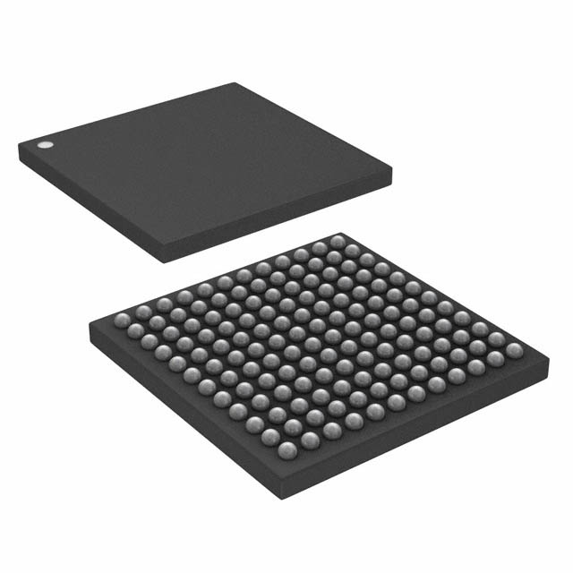
- Part No.:
- ADV212BBCZRL-150
- Manufacturer:
- Analog Devices Inc.
- Category:
- CODECS
- Package:
- 144-BGA, CSPBGA
- Datasheet:
-
 ADV212BBCZRL-150.pdf
- Description:
- IC CODEC VID JPEG 2000 144CSBGA
- Quantity:
- Payment:

- Shipping:

Inventory:2,227
Please send an inquiry. Send us your inquiry, and we will respond immediately.
Product details
Overview
ADV212BBCZRL-150 from Analog Devices is a JPEG2000-compatible video CODEC IC implementing wavelet-based compression/decompression for real-time video and high-resolution still images. It supports 9/7 (up to 1.048M-sample tiles) and 5/3 (up to 262K-sample tiles) wavelet transforms, operates at 150 MHz JCLK, and delivers ≤30% lower power than ADV202 in identical 144-ball CSP_BGA footprint. It targets professional digital video systems requiring ISO/IEC 15444-1 compliance and glueless ITU-R BT.656/SMPTE 274M interface.
For engineers reviewing the ADV212BBCZRL-150 datasheet, ADV212BBCZRL-150 pinout, ADV212BBCZRL-150 application, or ADV212BBCZRL-150 equivalent, this page provides verified technical context, validated pin functions, confirmed JPEG2000 feature coverage (excluding max-shift ROI), exact supply rail requirements (1.5 V core / 2.5 V or 3.3 V I/O), and real-world multichip HDTV scalability-enabling rapid integration into broadcast-grade encode/decode pipelines.
Technical Context
The ADV212BBCZRL-150 integrates a dedicated wavelet engine supporting both reversible (5/3) and irreversible (9/7) transforms up to 5 levels, three entropy CODECs compliant with JPEG2000 Part 1 (except maximum shift ROI), and an embedded RISC processor managing full code stream generation (J2C/JP2). Its internal DMA engine routes pixel data between VDATA and HDATA buses without host intervention.
It features dual asynchronous interfaces: a 16-bit SRAM-style host bus (HDATA[15:0], ADDR[3:0], CS, RD, WE, ACK) and a programmable video port (VDATA) supporting ITU-R BT.656, SMPTE 274M (1080i), SMPTE 296M (720p), PAL/NTSC, and raw pixel modes up to 65 MSPS (irreversible) or 40 MSPS (reversible).
Key Specifications
| Parameter | Value and Actual Design Meaning |
|---|---|
| JCLK Speed | 150 MHz - Enables full-rate processing of SMPTE 274M HDTV (1080i) in multichip configurations. |
| Core Supply | 1.5 V ±75 mV - Requires tight-regulation LDO; dynamic current up to 440 mA at 150 MHz. |
| I/O Supply | 2.5 V or 3.3 V - Configurable per board design; VIH/VIL thresholds differ per rail. |
| Wavelet Support | 9/7 (irreversible) and 5/3 (reversible) - Tile sizes: 1.048M samples (9/7) or 262K samples (5/3). |
| Video Input Rate | 65 MSPS (irreversible), 40 MSPS (reversible) - Matches SMPTE 274M line rates with margin. |
| Package | 13 mm × 13 mm, 144-ball CSP_BGA - Identical footprint to ADV202; θJA = 22.5°C/W. |
| JTAG Support | IEEE 1149.1 compliant - Enables boundary scan test and debug without halting operation. |
Pinout & Package
ADV212BBCZRL-150 uses a 13 mm × 13 mm, 144-ball CSP_BGA package (ball pitch: 0.8 mm), RoHS-compliant, rated for reflow at 260°C (20–40 sec). Thermal resistance: θJA = 22.5°C/W, θJC = 3.8°C/W.
| Pin/Terminal | Circuit Role | Design Meaning |
|---|---|---|
| MCLK | System clock input | Drives internal PLL; min 10 MHz, max 75.18 MHz; used for timing all internal operations. |
| RESET | Asynchronous reset input | Active-low; requires CS, RD, WE, DACK0/1, DREQ0/1 held high during assertion. |
| HDATA[15:0] | Host data bus (bidirectional) | 16-bit wide async SRAM interface; supports glueless connection to 16-/32-bit microcontrollers via HDATA[23:16] extension. |
| ADDR[3:0] | Host address bus | 4-bit address for register/FIFO access; enables direct/indirect register mapping and FIFO control. |
| CS | Chip select input | Qualifies all host read/write cycles; must be asserted before RD/WE and held until ACK deasserts. |
| RD / WE | Read/write strobes | Async control signals; RD active-low for reads, WE active-low for writes; support normal/DMA/streaming modes. |
| ACK | Operation acknowledge output | Indicates successful register access; not required for FIFO transfers under timing compliance. |
| VDATA[7:0] | Video data bus (bidirectional) | 8-bit parallel pixel/data path; supports ITU-R BT.656, SMPTE 274M, raw pixel, and JDATA streaming modes. |
| HSYNC / VSYNC / FIELD | Video timing control inputs/outputs | Synchronize pixel capture/display; polarity programmable; support CCIR 656 and HVF formats. |
Key Features
| Feature | Design Value |
|---|---|
| Patented SURF filtering | Enables low-power, hardware-accelerated wavelet decomposition without external memory bandwidth penalty. |
| Identical pinout to ADV202 | Allows drop-in replacement in existing ADV202 designs-no PCB or firmware changes required for basic functionality. |
| Flexible video interface | Supports SMPTE 274M (1080i), SMPTE 296M (720p), ITU-R BT.656, and custom raw pixel formats up to 65 MSPS. |
| Multichip scalability | Two or more ADV212BBCZRL-150 devices can be synchronized to encode/decode full-frame 1080i or 720p HDTV. |
| JTAG/boundary scan | Enables production test, in-system debug, and configuration verification without halting video pipeline operation. |
Applications
| Digital Cinema Encoding | Professional Video Editing |
|---|---|
Use Scenario: Real-time JPEG2000 compression of 4K RAW camera feeds for on-set dailies and archival. IC Role / Device Role / Timing Role: Primary encoder engine handling wavelet transform, quantization, and entropy coding; synchronized to camera pixel clock (≤65 MSPS). Use Value: Maintains visually lossless quality at 2.5:1–5:1 compression ratios while meeting SMPTE ST 2067-201 compliance for IMF packaging. |
Use Scenario: Hardware-accelerated decode of JP2 files during non-linear editing (NLE) timeline scrubbing and rendering. IC Role / Device Role / Timing Role: Dedicated decoder co-processor offloading CPU/GPU; accepts J2C streams over HDATA bus and outputs uncompressed YUV422 via VDATA. Use Value: Enables sub-frame latency (<10 ms) playback of multiple 1080p60 streams simultaneously without frame drops. |
| Digital CCTV Surveillance | Wireless Broadcast Contribution |
Use Scenario: Edge-based compression of multi-sensor panoramic video for low-bandwidth IP transmission. IC Role / Device Role / Timing Role: Standalone encoder interfaced to CMOS image sensors; uses 5/3 reversible mode for forensic-quality archiving. Use Value: Achieves 100% bit-exact reconstruction of critical evidence frames while reducing storage by 3× vs. MJPEG. |
Use Scenario: Mobile OB van encoding of live 1080i feeds for satellite uplink with minimal latency and robustness. IC Role / Device Role / Timing Role: Multichip encoder cluster (≥2 units) configured in master/slave mode for full-frame SMPTE 274M processing. Use Value: Delivers <50 ms end-to-end encode+transmit latency with error-resilient packetized J2C streams suitable for RF link instability. |
Equivalent & Alternatives
The following parts are listed as comparable options for similar JPEG2000 video codec applications.
| Alternative Part | Technical Difference | Application Difference | Selection Advice |
|---|---|---|---|
| ADV212BBCZ-115 | 121-ball CSP_BGA, 115 MHz JCLK speed grade; higher θJA (32.8°C/W); same core logic and pinout. | Lower throughput (max 40 MSPS reversible); suited for SDTV or cost-sensitive single-chip deployments. | Select when thermal budget permits higher junction temp or when 115 MHz suffices for target resolution/frame rate. |
| ADV202BBCZ-150 | No JTAG support; 30% higher dynamic power; identical 144-ball CSP_BGA footprint and register map. | Lacks boundary scan testability and power efficiency; functionally compatible but not upgradeable in field. | Choose only for legacy ADV202-based designs where JTAG is unnecessary and power dissipation is acceptable. |
Compared with ADV212BBCZ-115, the ADV212BBCZRL-150 delivers 31% higher clock frequency and 10.3°C/W lower thermal resistance-critical for sustained HDTV encoding. Against ADV202BBCZ-150, it adds JTAG and reduces power by ≥30%, enabling denser board layouts and cooler operation without changing PCB or firmware.
Availability
ADV212BBCZRL-150 is available at Aetrix Electronics and suitable for digital cinema encoding, professional video editing, digital CCTV surveillance, and wireless broadcast contribution requiring stable component supply across extended product lifecycles.
Supply support for ADV212BBCZRL-150 includes scheduled delivery planning, volume procurement assistance, BOM continuity management, traceable sourcing, and lifecycle availability coordination for OEM customers, industrial embedded developers, connected-device designers, and electronics production programs.
Manufacturer
Analog Devices, Inc. is a global semiconductor leader specializing in high-performance analog, mixed-signal, and digital signal processing technologies for precision instrumentation, communications, and industrial applications.
The ADV212BBCZRL-150 belongs to Analog Devices' Wavescale® video codec product line, designed specifically to offload JPEG2000 compression/decompression from host processors in broadcast, medical imaging, and defense video systems.
FAQ
What video standards does the ADV212BBCZRL-150 natively support?
The ADV212BBCZRL-150 directly supports ITU-R BT.656, SMPTE 125M, SMPTE 274M (1080i), SMPTE 296M (720p), SMPTE 293M (525p), and ITU-R BT.1358 (625p) via its dedicated VDATA interface. It also handles raw pixel formats up to 65 MSPS in irreversible mode. All timing parameters-including HSYNC/VSYNC setup/hold and sync delays-are fully specified in the datasheet for each standard, and the ADV212BBCZRL-150 requires no external framing logic to interface with compliant video sources.
Can the ADV212BBCZRL-150 generate fully compliant JPEG2000 code streams without host software intervention?
Yes, the ADV212BBCZRL-150 generates fully compliant ISO/IEC 15444-1 JPEG2000 code streams (J2C) and enhanced JP2 files autonomously using its embedded RISC processor and entropy CODECs. It supports all mandatory Part 1 features except maximum shift region-of-interest (ROI). Host involvement is optional-for example, to manage bit-rate control or inject metadata-but not required for baseline encoding/decoding functionality.
Is the ADV212BBCZRL-150 pin-compatible with the ADV202, and what modifications are needed for migration?
Yes, the ADV212BBCZRL-150 has identical pinout and footprint to the ADV202BBCZ-150 in the 144-ball CSP_BGA package. Migration requires no PCB changes. Firmware updates are optional: JTAG support and power reduction features are enabled by default, but legacy ADV202 register maps and timing sequences remain fully functional-making the ADV212BBCZRL-150 a true drop-in upgrade.
What are the power supply requirements for the ADV212BBCZRL-150, and how do they impact thermal design?
The ADV212BBCZRL-150 requires a 1.5 V ±75 mV core supply (VDD) delivering up to 440 mA at 150 MHz JCLK, and a separate 2.5 V or 3.3 V I/O supply (IOVDD) drawing up to 50 mA. Its 144-ball CSP_BGA package has θJA = 22.5°C/W. To maintain Tj < 105°C at 85°C ambient, total power dissipation must stay below 710 mW-achievable with proper copper pour, thermal vias, and airflow, especially given its ≥30% lower power versus ADV202.
How does multichip operation work for full-frame SMPTE 274M (1080i) encoding with the ADV212BBCZRL-150?
The ADV212BBCZRL-150 supports multichip encode/decode via synchronized VCLK and shared control signals. For SMPTE 274M (1080i), two units split the frame vertically: one processes top fields, the other bottom fields. The host configures master/slave mode using EDMOD registers, and the chips coordinate tile boundaries and code stream stitching internally-producing a single, fully compliant J2C file without external arbitration logic.
ADV212BBCZRL-150 Specifications
- Product attributes
- Attribute value
- Manufacturer:
- Analog Devices Inc.
- Series:
- Wavescale®
- Package/Case:
- 144-BGA, CSPBGA
- Packaging:
- Tape & Reel (TR)
- Product Status:
- Active
- Type:
- Video, JPEG2000
- Data Interface:
- -
- Resolution (Bits):
- 16 b
- Number of ADCs / DACs:
- -
- Sigma Delta:
- No
- S/N Ratio, ADCs / DACs (db) Typ:
- -
- Dynamic Range, ADCs / DACs (db) Typ:
- -
- Voltage - Supply, Analog:
- 1.5V, 3.3V
- Voltage - Supply, Digital:
- 1.5V, 3.3V
- Operating Temperature:
- -40°C ~ 85°C
- Grade:
- -
- Qualification:
- -
- Mounting Type:
- Surface Mount
- Supplier Device Package:
- 144-CSPBGA (13x13)
ADV212BBCZRL-150 FAQ
1.How can I place an order for ADV212BBCZRL-150 through Aetrix?
Please submit a Request for Quotation (RFQ) for ADV212BBCZRL-150 on Aetrix. Our sales agent will provide a competitive quotation and guide you through the order confirmation once you accept the terms.
2.Are the price and stock information for ADV212BBCZRL-150 reliable?
The price and inventory of ADV212BBCZRL-150 are updated periodically and may fluctuate due to market conditions. Stock and pricing data are typically refreshed every 24 hours. Quotation validity for ADV212BBCZRL-150 is usually 5 days.
3.What payment methods are accepted for ADV212BBCZRL-150?
We accept Wire Transfer, PayPal, Credit Card, Western Union, MoneyGram, and Escrow for ADV212BBCZRL-150 transactions.
Note: Certain payment methods may incur a processing fee.
4.How is shipping managed for ADV212BBCZRL-150?
ADV212BBCZRL-150 orders can be shipped via leading logistics carriers, including DHL, UPS, FedEx, TNT, or Registered Mail.
Once your ADV212BBCZRL-150 order is processed, you will receive an email with the shipment details and tracking number.
Note: Tracking information may take up to 24 hours to appear. Express delivery typically takes 3–5 business days.
5.How can I obtain technical support or documentation for ADV212BBCZRL-150?
For technical support, including ADV212BBCZRL-150 datasheets, pinout diagrams, or application guidance, please contact our engineering support team. They can provide detailed documentation and assistance for your ADV212BBCZRL-150 requirements.
6.How does Aetrix verify that ADV212BBCZRL-150 is sourced from the original manufacturer or authorized distributors?
All ADV212BBCZRL-150 products on Aetrix are procured from qualified distributors and authorized channels. Our dedicated quality assurance team conducts strict verification, including traceability checks and, if necessary, third-party testing. This ensures that ADV212BBCZRL-150 meets industry standards.
7.What is the process for return or replacement of ADV212BBCZRL-150?
All ADV212BBCZRL-150 units undergo pre-shipment inspection (PSI). If there is an issue with ADV212BBCZRL-150, returns or replacements are accepted under the following conditions:
1.Quantity discrepancies, incorrect items, or visible external defects (such as breakage or corrosion), acknowledged by Aetrix.
2.The issue is reported within 90 days of delivery.
3.The ADV212BBCZRL-150 part is unused and in its original packaging.
Return procedure for ADV212BBCZRL-150:
1.Submit a request within 90 days.
2.Obtain a Return Material Authorization (RMA) from Aetrix.
ADV212BBCZRL-150 Tags
-
NAU88C22YG
Nuvoton Technology Corporation

-
TLV320AIC3100IRHBR
Texas Instruments
-
DA7212-01UM2
Renesas
-
NAU8810YG
Nuvoton Technology Corporation
-
DA7218-00U32
Renesas
-
CMX655DQ6-TR1K
CML Micro
-
SGTL5000XNLA3
NXP Semiconductors
-
TLV320AIC3104IRHBR
Texas Instruments
-
MAX9867EWV+T
Analog Devices Inc./Maxim Integrated

-
MAX9860ETG+T
Analog Devices Inc./Maxim Integrated

-
TLV320AIC3106IRGZR
Texas Instruments
-
SGTL5000XNLA3R2
NXP Semiconductors
Tech Hub

A practical engineering guide to 3.3V and 5V logic compatibility, input thresholds, resistor dividers, translator ICs, MOSFET level shifting, I2C pull-ups, timing limits and power-sequencing risks.

The 74HC595 uses push-pull logic outputs, while the TPIC6B595 uses 50 V open-drain DMOS sinks for higher-power loads. This guide compares timing, current limits, 3.3 V interfacing, load wiring, thermal…

The 74HC595 converts serial data into eight stable parallel outputs. This guide covers pin functions, shift and storage timing, OE and MR behavior, drive-current limits, cascading, voltage compatibilit…

A technical comparison of level-sensitive latches and edge-triggered flip-flops, covering timing windows, setup and hold limits, master–slave operation, time borrowing, race-through, HDL inference and…

A D latch stores one bit while Enable controls when data can pass. This reference covers gate-level operation, truth tables, transparency, setup and hold timing, LE versus OE, common ICs and practical …

An SR latch stores one bit through cross-coupled feedback. This engineering reference covers NOR and NAND implementations, truth tables, forbidden-state recovery, gated operation, switch debouncing, fa…

Latch circuits retain one bit through feedback. This technical reference covers SR and D latches, truth tables, transparency, timing limits, latch-versus-flip-flop behavior, applications and common log…

An engineering guide to LED driver operation, constant-current and constant-voltage outputs, linear and switching topologies, dimming, IC selection, calculations, replacement compatibility, and fault c…

Operational amplifier guide covering op amp basics, feedback, ideal vs real op amps, common configurations, buffer circuits, offset, bias current, gain-bandwidth, slew rate, rail-to-rail limits and sel…

Jumper cables guide covering safe connection order, red and black clamp placement, final ground connection, cable gauge, length, clamp quality, copper vs CCA cables, jump starter comparison and battery…


