
 My Inquiry
 My Account


Analog Devices Inc. ADV476KN80E
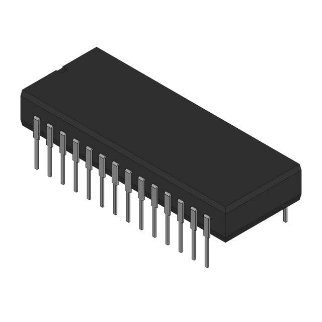
- Part No.:
- ADV476KN80E
- Manufacturer:
- Analog Devices Inc.
- Category:
- Digital to Analog Converters (DAC)
- Package:
- 28-DIP (0.600", 15.24mm)
- Datasheet:
-
 ADV476KN80E.pdf
- Description:
- IC DAC 6BIT A-OUT 28DIP
- Quantity:
- Payment:

- Shipping:

Inventory:5,648
Please send an inquiry. Send us your inquiry, and we will respond immediately.
Product details
Overview
ADV476KN80E from Analog Devices is a monolithic CMOS RGB palette RAM-DAC designed for VGA and IBM Personal System/2 color graphics systems. It integrates a 256×18-bit color lookup table, triple 6-bit D/A converters, and asynchronous MPU interface, delivering RS-343A/RS-170–compliant analog outputs at up to 66 MHz pixel clock rate for high-resolution color display generation.
For engineers reviewing the ADV476KN80E datasheet, ADV476KN80E pinout, ADV476KN80E application, or ADV476KN80E equivalent, this device supports real-time palette updates during vertical blanking, pixel-level masking for animation overlays, and direct coaxial cable drive without external buffers - critical for legacy graphics controller design and retro-computing video subsystems.
Technical Context
The ADV476KN80E implements a pipelined 66 MHz architecture with independent pixel clock (PCLK) and MPU bus domains. Its 256-entry × 18-bit palette RAM stores three 6-bit RGB components per address, accessed via P0–P7 pixel select inputs or MPU-controlled RS0/RS1 command decoding.
Each of the three current-output DACs delivers up to 19.05 mA into 37.5 Ω (doubly terminated 75 Ω), with guaranteed monotonicity and ±0.5 LSB integral nonlinearity. The BLANK input latches on PCLK's rising edge to force all outputs to black level, enabling precise sync timing in raster-scan CRT systems.
Key Specifications
| Parameter | Value and Actual Design Meaning |
|---|---|
| Resolution | 6-bit per DAC channel - defines 64 discrete intensity levels per primary color (RGB) |
| Max Pixel Clock | 66 MHz - supports up to 1280×1024 @ 72 Hz or 1024×768 @ 85 Hz VGA timing |
| Palette Size | 256 × 18-bit - enables simultaneous display of 256 colors selected from 262,144 total addressable colors |
| Analog Output Type | High-impedance current sources - directly drive doubly terminated 75 Ω coaxial cables per RGB channel |
| MPU Interface | Asynchronous 8-bit bidirectional bus with RS0/RS1 addressing - eliminates need for external address multiplexers |
| Blank Control | TTL-compatible BLANK input - forces RGB outputs to black level synchronously with PCLK edge |
| Power Supply | +5 V ±10% CMOS supply - draws ≤220 mA at 66 MHz, enabling integration into low-noise analog/digital partitioned PCB layouts |
Pinout & Package
ADV476KN80E is packaged in a 28-pin plastic DIP (N-28), 0.6" wide, with dual analog/digital power and ground pins optimized for noise isolation in mixed-signal video applications.
| Pin/Terminal | Circuit Role | Design Meaning |
|---|---|---|
| P0–P7 | Pixel address inputs | Latched on PCLK rising edge to select one of 256 palette entries for current RGB output |
| RED, GREEN, BLUE | Analog current outputs | High-Z current sources (max 19.05 mA) - each drives 37.5 Ω load for RS-343A video levels |
| BLANK | Composite blank control | TTL input that forces all RGB outputs to black level when logic low; synchronized to PCLK |
| PCLK | Pixel clock input | Rising edge latches P0–P7 and BLANK - defines video sampling rate and frame timing boundary |
| D0–D7 | MPU data bus | Bidirectional 8-bit interface for palette RAM writes/reads and address register access |
| WR / RD | Write/read strobes | TTL-compatible controls for MPU-initiated palette or register access - operate asynchronously to PCLK |
| RS0, RS1 | Command decode inputs | Select MPU operation mode: address register, palette RAM, or pixel read mask register |
| IREF | Current reference input | Sets full-scale DAC output (e.g., 8.88 mA → 0.714 V across 37.5 Ω for RS-343A compliance) |
Key Features
| Feature | Design Value |
|---|---|
| VGA & PS/2 software compatibility | Pin- and register-level identical to INMOS 171/176 - enables drop-in replacement in legacy graphics controllers |
| Pixel read mask register | Enables bitwise AND of P0–P7 with mask value - allows dynamic color plane partitioning for animation without palette reload |
| Asynchronous MPU access | Allows palette updates during vertical blanking while video stream runs uninterrupted - no frame tearing or timing disruption |
| RS-343A/RS-170 compliant outputs | Direct drive capability eliminates external op-amps or buffers - reduces BOM count and layout complexity in CRT monitor interfaces |
| Guaranteed monotonic DACs | ±0.5 LSB integral linearity ensures smooth grayscale ramps and absence of visual banding in gradient displays |
Applications
| High Resolution Color Graphics | CAE/CAD/CAM Systems |
|---|---|
Use Scenario: Driving analog RGB inputs of 1024×768 CRT monitors in engineering workstations. IC Role / Device Role / Timing Role: Palette RAM-DAC translating digital pixel indices into analog RGB video signals synchronized to PCLK. Use Value: Enables real-time palette reprogramming during vertical blanking to support multi-layer CAD overlays without frame corruption. | Use Scenario: Rendering complex wireframe models with color-coded topology on legacy UNIX graphics terminals. IC Role / Device Role / Timing Role: Video output engine converting framebuffer pixel values into calibrated RGB currents compliant with RS-343A standards. Use Value: Delivers 66 MHz pixel throughput and ±0.5 LSB DAC linearity to preserve fine detail and avoid contouring artifacts in technical drawings. |
| Image Processing Workstations | Desktop Publishing Systems |
Use Scenario: Real-time false-color mapping of medical or satellite imagery on diagnostic displays. IC Role / Device Role / Timing Role: Dynamic palette loader using pixel read mask register to apply color LUTs per scanline without CPU intervention. Use Value: Reduces host processor load by offloading pixel-level masking - enables 30+ fps full-screen image updates on 80386-class systems. | Use Scenario: Generating WYSIWYG RGB previews of PostScript documents on prepress proofing monitors. IC Role / Device Role / Timing Role: High-fidelity RGB signal generator with stable 0.714 V white level and black-level accuracy within ±0.5 LSB. Use Value: Ensures consistent color reproduction across print proofs by maintaining tight DAC matching (±2.5% between RGB channels). |
Equivalent & Alternatives
The following parts are listed as comparable options for similar RGB palette DAC applications.
| Alternative Part | Technical Difference | Application Difference | Selection Advice |
|---|---|---|---|
| ADV478KP66 | 44-pin PLCC package; adds voltage-reference mode via VREF pin; same 66 MHz speed and 256×18 palette | Requires different PCB footprint and decoupling layout; supports both current- and voltage-reference configurations | Select when board space permits larger PLCC and dual-reference flexibility is needed for system-level calibration |
| INMOS 176-066 | Original pin-compatible predecessor; identical 66 MHz timing but higher power draw (300 mA vs. 220 mA) and no BLANK synchronization guarantee | Legacy sourcing only; lacks documented monotonicity and glitch energy specs of ADV476 series | Use only for exact form-fit-function replacement where original INMOS stock remains available |
Compared with ADV476KN80E, the ADV478KP66 offers expanded reference configuration options at the cost of larger footprint and layout complexity, while the INMOS 176-066 provides mechanical compatibility but lacks modern DAC performance guarantees and power efficiency.
Availability
ADV476KN80E is available at Aetrix Electronics and suitable for high-resolution color graphics, CAE/CAD/CAM systems, and legacy instrumentation requiring stable component supply and long-term obsolescence management.
Supply support for ADV476KN80E includes scheduled delivery planning, volume procurement assistance, BOM continuity management, traceable sourcing, and lifecycle availability coordination for OEM customers, industrial embedded developers, connected-device designers, and electronics production programs.
Manufacturer
Analog Devices, Inc. is a U.S.-based semiconductor company specializing in high-performance analog, mixed-signal, and digital signal processing technologies.
The ADV476KN80E belongs to Analog Devices' legacy video interface product line, engineered specifically for VGA and IBM PS/2 color graphics subsystems requiring integrated palette RAM and triple DAC functionality in compact monolithic form.
FAQ
What is the maximum supported pixel clock frequency for the ADV476KN80E?
The ADV476KN80E is rated for 66 MHz pipelined operation, matching the highest speed grade in the ADV476 family. This enables support for resolutions such as 1024×768 at 85 Hz refresh or 1280×1024 at 72 Hz under standard VGA timing constraints. The device maintains guaranteed timing margins (e.g., t12 = 15.3 ns min setup) and full-spec performance including ±0.5 LSB linearity and 75 pV·sec glitch impulse at this rate. ADV476KN80E operates reliably across 0°C to +70°C ambient temperature with proper decoupling and layout per Analog Devices' PCB guidelines.
Does the ADV476KN80E support both current-mode and voltage-mode reference inputs?
No - the ADV476KN80E supports current-mode reference only via the IREF pin, requiring an external current source (e.g., LM334) set to 8.88 mA for RS-343A compliance. Voltage-reference operation is not supported on this 28-pin DIP variant. That capability is exclusive to the 44-pin PLCC versions (e.g., ADV476KP66 and ADV478KP66), which include dedicated VREF and COMP pins. ADV476KN80E's IREF input accepts –3 mA to –10 mA, with full-scale output voltage determined by VO = 2.15 × IREF × RL.
How does the pixel read mask register function in the ADV476KN80E?
The pixel read mask register performs bitwise logical AND between incoming P0–P7 pixel data and an 8-bit mask value loaded via the MPU interface. This enables dynamic color plane reduction - for example, masking upper bits to create animated overlays or flashing UI elements without modifying the main palette RAM. The mask register is accessible at RS0=1, RS1=0 and operates transparently during active video; ADV476KN80E applies it synchronously with PCLK, ensuring pixel-accurate timing. Its use eliminates CPU overhead associated with palette reloading during screen updates.
Can the ADV476KN80E drive standard 75 Ω coaxial video cables directly?
Yes - the ADV476KN80E's RED, GREEN, and BLUE outputs are high-impedance current sources capable of directly driving doubly terminated 75 Ω coaxial cables (i.e., 37.5 Ω source termination). When loaded with 37.5 Ω, each channel delivers 0.714 V peak-to-peak for RS-343A compliance or 1.0 V for RS-170, with typical output current of 19.05 mA at full scale. No external buffers or amplifiers are required, reducing system component count and signal path distortion. ADV476KN80E maintains <75 pV·sec glitch impulse and –35 dB clock feedthrough under these conditions.
What MPU bus protocols and timing modes does the ADV476KN80E support?
The ADV476KN80E supports asynchronous 8-bit MPU access using standard RD/WR strobes and RS0/RS1 command encoding. It implements four distinct operations: address register write/read (RS1=0,RS0=0 or RS1=1,RS0=1), palette RAM access (RS1=0,RS0=1), and pixel read mask register access (RS1=1,RS0=0). All timing parameters - including t4 (RD to data valid, 40 ns max), t6 (RD negated to high-Z, 10 ns min), and t8 (WR pulse width, 50 ns min) - are fully specified for 66 MHz operation. ADV476KN80E requires no wait states and operates independently of PCLK, enabling palette updates during vertical blanking without disrupting video output.
ADV476KN80E Specifications
- Product attributes
- Attribute value
- Manufacturer:
- Analog Devices Inc.
- Series:
- ADV476
- Package/Case:
- 28-DIP (0.600", 15.24mm)
- Packaging:
- Bulk
- Product Status:
- Active
- Programmable:
- Not Verified
- Number of Bits:
- 6
- Number of D/A Converters:
- 3
- Settling Time:
- -
- Output Type:
- Current - Unbuffered
- Differential Output:
- No
- Data Interface:
- -
- Reference Type:
- -
- Voltage - Supply, Analog:
- 4.5V ~ 5.5V
- Voltage - Supply, Digital:
- 4.5V ~ 5.5V
- INL/DNL (LSB):
- ±0.5 (Max), ±1 (Max)
- Architecture:
- -
- Operating Temperature:
- 0°C ~ 70°C
- Supplier Device Package:
- 28-PDIP
- Mounting Type:
- Through Hole
- Grade:
- -
- Qualification:
- -
ADV476KN80E FAQ
1.How can I place an order for ADV476KN80E through Aetrix?
Please submit a Request for Quotation (RFQ) for ADV476KN80E on Aetrix. Our sales agent will provide a competitive quotation and guide you through the order confirmation once you accept the terms.
2.Are the price and stock information for ADV476KN80E reliable?
The price and inventory of ADV476KN80E are updated periodically and may fluctuate due to market conditions. Stock and pricing data are typically refreshed every 24 hours. Quotation validity for ADV476KN80E is usually 5 days.
3.What payment methods are accepted for ADV476KN80E?
We accept Wire Transfer, PayPal, Credit Card, Western Union, MoneyGram, and Escrow for ADV476KN80E transactions.
Note: Certain payment methods may incur a processing fee.
4.How is shipping managed for ADV476KN80E?
ADV476KN80E orders can be shipped via leading logistics carriers, including DHL, UPS, FedEx, TNT, or Registered Mail.
Once your ADV476KN80E order is processed, you will receive an email with the shipment details and tracking number.
Note: Tracking information may take up to 24 hours to appear. Express delivery typically takes 3–5 business days.
5.How can I obtain technical support or documentation for ADV476KN80E?
For technical support, including ADV476KN80E datasheets, pinout diagrams, or application guidance, please contact our engineering support team. They can provide detailed documentation and assistance for your ADV476KN80E requirements.
6.How does Aetrix verify that ADV476KN80E is sourced from the original manufacturer or authorized distributors?
All ADV476KN80E products on Aetrix are procured from qualified distributors and authorized channels. Our dedicated quality assurance team conducts strict verification, including traceability checks and, if necessary, third-party testing. This ensures that ADV476KN80E meets industry standards.
7.What is the process for return or replacement of ADV476KN80E?
All ADV476KN80E units undergo pre-shipment inspection (PSI). If there is an issue with ADV476KN80E, returns or replacements are accepted under the following conditions:
1.Quantity discrepancies, incorrect items, or visible external defects (such as breakage or corrosion), acknowledged by Aetrix.
2.The issue is reported within 90 days of delivery.
3.The ADV476KN80E part is unused and in its original packaging.
Return procedure for ADV476KN80E:
1.Submit a request within 90 days.
2.Obtain a Return Material Authorization (RMA) from Aetrix.
ADV476KN80E Tags
-
MCP47A1T-A0E/LT
Microchip Technology

-
MCP4706A0T-E/CH
Microchip Technology
-
MCP4716A0T-E/MAY
Microchip Technology
-
MCP4716A0T-E/CH
Microchip Technology
-
MCP4726A0T-E/CH
Microchip Technology
-
MCP4725A0T-E/CH
Microchip Technology
-
MCP4725A1T-E/CH
Microchip Technology
-
MCP4725A2T-E/CH
Microchip Technology
-
MCP4726A1T-E/CH
Microchip Technology
-
MCP4726A3T-E/CH
Microchip Technology
-
MCP4726A2T-E/CH
Microchip Technology
-
MCP4726A0T-E/MAY
Microchip Technology
Tech Hub

A practical engineering guide to 3.3V and 5V logic compatibility, input thresholds, resistor dividers, translator ICs, MOSFET level shifting, I2C pull-ups, timing limits and power-sequencing risks.

The 74HC595 uses push-pull logic outputs, while the TPIC6B595 uses 50 V open-drain DMOS sinks for higher-power loads. This guide compares timing, current limits, 3.3 V interfacing, load wiring, thermal…

The 74HC595 converts serial data into eight stable parallel outputs. This guide covers pin functions, shift and storage timing, OE and MR behavior, drive-current limits, cascading, voltage compatibilit…

A technical comparison of level-sensitive latches and edge-triggered flip-flops, covering timing windows, setup and hold limits, master–slave operation, time borrowing, race-through, HDL inference and…

A D latch stores one bit while Enable controls when data can pass. This reference covers gate-level operation, truth tables, transparency, setup and hold timing, LE versus OE, common ICs and practical …

An SR latch stores one bit through cross-coupled feedback. This engineering reference covers NOR and NAND implementations, truth tables, forbidden-state recovery, gated operation, switch debouncing, fa…

Latch circuits retain one bit through feedback. This technical reference covers SR and D latches, truth tables, transparency, timing limits, latch-versus-flip-flop behavior, applications and common log…

An engineering guide to LED driver operation, constant-current and constant-voltage outputs, linear and switching topologies, dimming, IC selection, calculations, replacement compatibility, and fault c…

Operational amplifier guide covering op amp basics, feedback, ideal vs real op amps, common configurations, buffer circuits, offset, bias current, gain-bandwidth, slew rate, rail-to-rail limits and sel…

Jumper cables guide covering safe connection order, red and black clamp placement, final ground connection, cable gauge, length, clamp quality, copper vs CCA cables, jump starter comparison and battery…


