
 My Inquiry
 My Account


Analog Devices Inc. ADV601LCJST
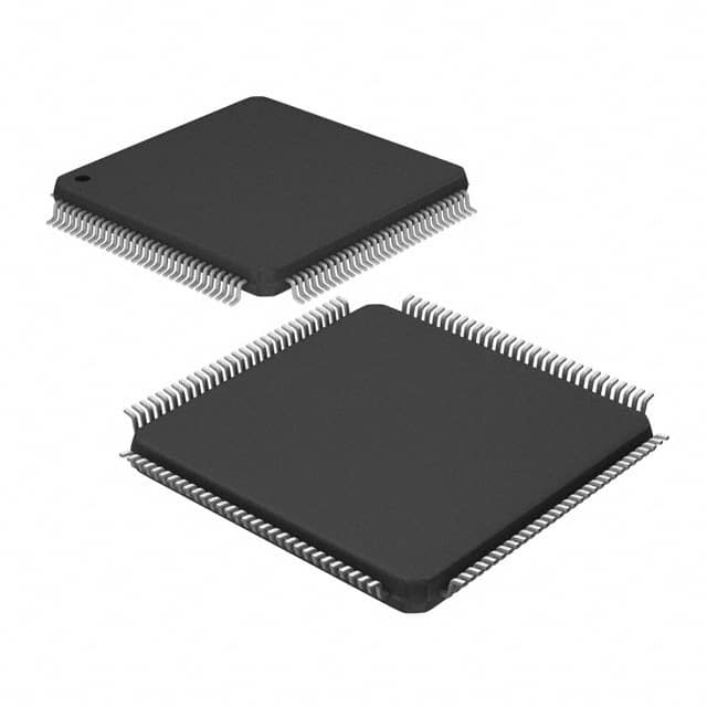
- Part No.:
- ADV601LCJST
- Manufacturer:
- Analog Devices Inc.
- Category:
- CODECS
- Package:
- 120-LQFP
- Datasheet:
-
 ADV601LCJST.pdf
- Description:
- IC CODEC VIDEO DSP/SRL 120LQFP
- Quantity:
- Payment:

- Shipping:

Inventory:2,703
Please send an inquiry. Send us your inquiry, and we will respond immediately.
Product details
Overview
ADV601LCJST from Analog Devices is a dedicated, single-chip, all-digital CMOS VLSI video encoder/decoder optimized for real-time interlaced digital video compression and decompression. It supports CCIR-601 input at 720×243@60 Hz (NTSC) and 720×288@50 Hz (PAL), delivers visually loss-less compression at 4:1 on natural images, and achieves compression ratios up to 350:1. It integrates glueless 8-bit CCIR-656 video interface and 16-/32-bit host interface with 512-deep 32-bit FIFO - used in PC video editing and remote CCTV surveillance systems.
For engineers reviewing the ADV601LCJST datasheet, ADV601LCJST pinout, ADV601LCJST application, or ADV601LCJST equivalent, key selection considerations include field-independent sub-band coding architecture, bi-orthogonal (7,9) wavelet transform, adaptive quantizer bin-width control via external DSP/host, real-time interlaced video processing capability, and compatibility with external 256K × 16-bit DRAM for field storage.
Technical Context
The ADV601LCJST implements field-independent sub-band coding using a bi-orthogonal (7,9) wavelet kernel that performs separable 2D transforms without block partitioning - eliminating DCT-style blocking artifacts. Its on-chip transform buffer provides SRAM-based delay-line storage for full-image wavelet computation, removing need for ultra-fast external memory.
Compression is achieved through programmable quantization of wavelet coefficients based on human visual system response, followed by run-length and fixed-table Huffman coding. Quantizer bin-width parameters are computed externally and loaded via host interface; during decode, bin widths are extracted directly from the compressed bit stream.
Key Specifications
| Parameter | Value and Actual Design Meaning |
|---|---|
| Video Standard Support | CCIR-601/525 (720×[email protected] Hz) and CCIR-601/625 (720×288@50 Hz); no progressive-scan support. |
| Max Pixel Rate | 13.5 MHz - defines maximum video bandwidth compatible with internal timing and DRAM manager. |
| Compression Ratio Range | Visually loss-less to 350:1 - selectable per application; 4:1 yields typical visually loss-less quality on natural images. |
| Host Interface Width | 16- or 32-bit parallel - supports glueless connection to microprocessors, DSPs, or bridge logic for PCI/ISA/SCSI. |
| FIFO Depth | 512 × 32-bit entries - buffers compressed video data between Huffman coder and host, smoothing bursty transfers. |
| External Memory Requirement | 256K × 16-bit DRAM - used exclusively for field storage; managed autonomously by on-chip DRAM manager. |
| Video Interface Format | 8-bit multiplexed CCIR-656 or Philips formats - supports YCbCr 4:2:2 component digital video with embedded sync. |
Pinout & Package
ADV601LCJST is housed in a 100-lead LQFP (Low-Profile Quad Flat Package) with 0.5 mm pitch, body size 14 mm × 14 mm, and standard JEDEC MO-152AC footprint. Thermal pad exposed on underside for enhanced heat dissipation in video-processing applications.
| Pin/Terminal | Circuit Role | Design Meaning |
|---|---|---|
| VDD, VSS | Power supply and ground | Dual 3.3 V supply domains: core logic (VDDC) and I/O (VDDIO); separate analog/digital grounds required per layout guidelines. |
| CLKIN | Master clock input | Accepts 13.5 MHz or 27 MHz crystal or oscillator; drives internal PLL generating video and host timing domains. |
| HCLK, HRESET | Host interface clock/reset | Synchronous 16-/32-bit parallel bus control; HRESET initializes register map and FIFO state. |
| HD[15:0], HD[31:0] | Host data bus | Bidirectional multiplexed data path; width selected via MODE pins; auto-incrementing address mode supported for bulk register access. |
| VID[7:0] | Video data input/output | 8-bit bidirectional port carrying time-multiplexed Y/Cb/Cr samples in CCIR-656 format with embedded sync codes. |
| HIRQ, STATS_R, LCODE, FIFO_SRQ | Interrupt and status outputs | Open-drain active-low signals indicating statistics ready, last code read, FIFO service request, and error conditions. |
| DRAM_A[17:0], DRAM_DQ[15:0] | External DRAM interface | Dedicated 18-bit address and 16-bit data bus; fully managed by on-chip DRAM controller - no external address generation logic needed. |
Key Features
| Feature | Design Value |
|---|---|
| Field-independent wavelet coding | Processes each video field as independent unit - enables seamless frame-rate conversion and avoids inter-field motion artifacts. |
| Bi-orthogonal (7,9) wavelet kernel | Provides superior energy compaction vs. DCT; eliminates blocking artifacts and enables graceful degradation at high compression. |
| On-chip transform buffer | SRAM-based delay line eliminates need for external high-speed memory - reduces BOM count and PCB routing complexity. |
| Adaptive quantizer with external BW control | Bin-width parameters calculated off-chip allow real-time bit-rate stabilization across scene changes without sacrificing quality. |
| Glueless CCIR-656 interface | Direct connection to video decoders/encoders (e.g., AD72xx, SAA71xx) without level shifters or timing glue logic. |
Applications
| PC Video Editing | Remote CCTV Surveillance |
|---|---|
Use Scenario: Real-time capture and playback of uncompressed DV streams on x86-based workstations with ISA/PCI host interface. IC Role / Device Role / Timing Role: Dedicated video codec performing encode/decode in hardware - offloads CPU, enables software-based nonlinear editing with low latency. Use Value: Enables 4:1 visually loss-less compression while maintaining CCIR-601 fidelity - reduces storage bandwidth by 75% without perceptible quality loss. | Use Scenario: Low-bandwidth transmission of PAL/NTSC video over leased lines or early DSL links in security monitoring centers. IC Role / Device Role / Timing Role: Field-synchronized encoder generating constant-bit-rate streams via external DSP-controlled bin-width adaptation. Use Value: Delivers stable 1–2 Mbps output for 720×288@50 Hz - fits within narrowband telecom channels while preserving motion detail. |
| Digital Camcorders | TV Instant Replay |
Use Scenario: Embedded recording subsystem in portable camcorders using flash or miniDV tape with limited power and space budget. IC Role / Device Role / Timing Role: Low-power, single-chip video compression engine interfacing directly to CCD sensor output and host controller. Use Value: Achieves 350:1 max compression ratio - extends recording time on fixed media while retaining usable image resolution for playback. | Use Scenario: Broadcast studio replay server capturing live NTSC feeds for instant slow-motion playback during sports events. IC Role / Device Role / Timing Role: High-reliability encode/decode pipeline synchronized to genlock reference, supporting frame-accurate seek and variable-speed playback. Use Value: Field-independent processing ensures zero interlace artifacts during freeze-frame and slow-motion - critical for broadcast compliance. |
Equivalent & Alternatives
The following parts are listed as comparable options for similar video codec applications.
| Alternative Part | Technical Difference | Application Difference | Selection Advice |
|---|---|---|---|
| ADV601JST | Pin-compatible but higher-cost variant; includes extended temperature range (–40°C to +85°C) and tighter AC specs. | Required for industrial or automotive environments where thermal stability exceeds ADV601LCJST's 0°C to +70°C rating. | Select ADV601JST only when extended temperature operation or guaranteed AC performance across full range is mandatory. |
| Brooktree Bt819 | Integrated video decoder + encoder; lacks wavelet compression - uses proprietary DCT-based algorithm with lower max compression (100:1). | Used in legacy Windows CE-based DVRs requiring analog composite/S-video input instead of digital CCIR-656. | Choose Bt819 only when analog video source integration is needed and wavelet-based artifact-free compression is not required. |
Compared with ADV601JST, the ADV601LCJST trades extended temperature tolerance and tighter timing margins for lower cost and identical core functionality; compared with Bt819, it offers superior compression efficiency and digital-native interface but requires external video digitization.
Availability
ADV601LCJST is available at Aetrix Electronics and suitable for PC video editing, remote CCTV surveillance, and digital camcorder designs requiring stable component supply, long-term lifecycle support, and verified second-source alternatives.
Supply support for ADV601LCJST includes scheduled delivery planning, volume procurement assistance, BOM continuity management, traceable sourcing, and lifecycle availability coordination for OEM customers, industrial embedded developers, connected-device designers, and electronics production programs.
Manufacturer
Analog Devices, Inc. is a global semiconductor company specializing in high-performance analog, mixed-signal, and digital signal processing ICs for precision instrumentation, communications, and industrial applications.
The ADV601LC product line was designed specifically for cost-sensitive, real-time interlaced video compression in consumer and professional digital video equipment - emphasizing minimal external components, field-level processing, and seamless integration with standard video interfaces.
FAQ
What video standards does the ADV601LCJST support?
The ADV601LCJST supports CCIR-601/525 (720×[email protected] Hz, NTSC) and CCIR-601/625 (720×288@50 Hz, PAL) interlaced digital video formats only. It does not support progressive scan, HDMI, SDI, or analog inputs. The device requires CCIR-656-compliant 8-bit multiplexed YCbCr 4:2:2 video with embedded sync codes, and its internal timing is locked to 13.5 MHz pixel clock.
Is the ADV601LCJST pin-compatible with the ADV601?
Yes, the ADV601LCJST is 100% bitstream compatible and pin-compatible with the ADV601. Both share identical pin configuration, register map, timing behavior, and functional block diagram. The "LC" suffix denotes the ultralow-cost variant with identical architecture but optimized for reduced manufacturing cost - no PCB redesign or firmware changes are needed when migrating from ADV601 to ADV601LCJST.
Does the ADV601LCJST require external DRAM, and what type?
Yes, the ADV601LCJST requires one 256K × 16-bit DRAM (e.g., MT48LC16M16A2) for field storage, managed entirely by its on-chip DRAM controller. The DRAM interface uses dedicated 18-bit address and 16-bit data buses with no external address generation logic required. The device supports standard asynchronous DRAM with 60 ns access time and automatic refresh control.
How does the ADV601LCJST achieve constant bit rate during encoding?
The ADV601LCJST achieves near-constant bit rate by accepting externally calculated bin-width parameters from a host DSP or processor. These parameters - derived from field statistics (e.g., sum-of-squares, min/max luma) - adjust quantization granularity per Mallat sub-band in real time. The ADV601LCJST provides STATSR and LCODE interrupts to synchronize this adaptive control loop without interrupting video flow.
What is the role of the on-chip transform buffer in the ADV601LCJST?
The on-chip transform buffer in the ADV601LCJST is a dedicated SRAM array used exclusively by the wavelet kernel to store intermediate results during 2D separable wavelet transforms. It eliminates reliance on external high-speed memory for transform computation, enabling full-image filtering without block partitioning - a key factor in avoiding DCT-style blocking artifacts and reducing system-level BOM count.
ADV601LCJST Specifications
- Product attributes
- Attribute value
- Manufacturer:
- Analog Devices Inc.
- Series:
- -
- Package/Case:
- 120-LQFP
- Packaging:
- Bag
- Product Status:
- Obsolete
- Type:
- Video Codec
- Data Interface:
- DSP, Serial
- Resolution (Bits):
- 8 b
- Number of ADCs / DACs:
- -
- Sigma Delta:
- No
- S/N Ratio, ADCs / DACs (db) Typ:
- -
- Dynamic Range, ADCs / DACs (db) Typ:
- -
- Voltage - Supply, Analog:
- 4.5V ~ 5.5V
- Voltage - Supply, Digital:
- 4.5V ~ 5.5V
- Operating Temperature:
- 0°C ~ 70°C
- Grade:
- -
- Qualification:
- -
- Mounting Type:
- Surface Mount
- Supplier Device Package:
- 120-LQFP (14x14)
ADV601LCJST FAQ
1.How can I place an order for ADV601LCJST through Aetrix?
Please submit a Request for Quotation (RFQ) for ADV601LCJST on Aetrix. Our sales agent will provide a competitive quotation and guide you through the order confirmation once you accept the terms.
2.Are the price and stock information for ADV601LCJST reliable?
The price and inventory of ADV601LCJST are updated periodically and may fluctuate due to market conditions. Stock and pricing data are typically refreshed every 24 hours. Quotation validity for ADV601LCJST is usually 5 days.
3.What payment methods are accepted for ADV601LCJST?
We accept Wire Transfer, PayPal, Credit Card, Western Union, MoneyGram, and Escrow for ADV601LCJST transactions.
Note: Certain payment methods may incur a processing fee.
4.How is shipping managed for ADV601LCJST?
ADV601LCJST orders can be shipped via leading logistics carriers, including DHL, UPS, FedEx, TNT, or Registered Mail.
Once your ADV601LCJST order is processed, you will receive an email with the shipment details and tracking number.
Note: Tracking information may take up to 24 hours to appear. Express delivery typically takes 3–5 business days.
5.How can I obtain technical support or documentation for ADV601LCJST?
For technical support, including ADV601LCJST datasheets, pinout diagrams, or application guidance, please contact our engineering support team. They can provide detailed documentation and assistance for your ADV601LCJST requirements.
6.How does Aetrix verify that ADV601LCJST is sourced from the original manufacturer or authorized distributors?
All ADV601LCJST products on Aetrix are procured from qualified distributors and authorized channels. Our dedicated quality assurance team conducts strict verification, including traceability checks and, if necessary, third-party testing. This ensures that ADV601LCJST meets industry standards.
7.What is the process for return or replacement of ADV601LCJST?
All ADV601LCJST units undergo pre-shipment inspection (PSI). If there is an issue with ADV601LCJST, returns or replacements are accepted under the following conditions:
1.Quantity discrepancies, incorrect items, or visible external defects (such as breakage or corrosion), acknowledged by Aetrix.
2.The issue is reported within 90 days of delivery.
3.The ADV601LCJST part is unused and in its original packaging.
Return procedure for ADV601LCJST:
1.Submit a request within 90 days.
2.Obtain a Return Material Authorization (RMA) from Aetrix.
ADV601LCJST Tags
-
NAU88C22YG
Nuvoton Technology Corporation

-
TLV320AIC3100IRHBR
Texas Instruments
-
DA7212-01UM2
Renesas
-
NAU8810YG
Nuvoton Technology Corporation
-
DA7218-00U32
Renesas
-
CMX655DQ6-TR1K
CML Micro
-
SGTL5000XNLA3
NXP Semiconductors
-
TLV320AIC3104IRHBR
Texas Instruments
-
MAX9867EWV+T
Analog Devices Inc./Maxim Integrated

-
MAX9860ETG+T
Analog Devices Inc./Maxim Integrated

-
TLV320AIC3106IRGZR
Texas Instruments
-
SGTL5000XNLA3R2
NXP Semiconductors
Tech Hub

A practical engineering guide to 3.3V and 5V logic compatibility, input thresholds, resistor dividers, translator ICs, MOSFET level shifting, I2C pull-ups, timing limits and power-sequencing risks.

The 74HC595 uses push-pull logic outputs, while the TPIC6B595 uses 50 V open-drain DMOS sinks for higher-power loads. This guide compares timing, current limits, 3.3 V interfacing, load wiring, thermal…

The 74HC595 converts serial data into eight stable parallel outputs. This guide covers pin functions, shift and storage timing, OE and MR behavior, drive-current limits, cascading, voltage compatibilit…

A technical comparison of level-sensitive latches and edge-triggered flip-flops, covering timing windows, setup and hold limits, master–slave operation, time borrowing, race-through, HDL inference and…

A D latch stores one bit while Enable controls when data can pass. This reference covers gate-level operation, truth tables, transparency, setup and hold timing, LE versus OE, common ICs and practical …

An SR latch stores one bit through cross-coupled feedback. This engineering reference covers NOR and NAND implementations, truth tables, forbidden-state recovery, gated operation, switch debouncing, fa…

Latch circuits retain one bit through feedback. This technical reference covers SR and D latches, truth tables, transparency, timing limits, latch-versus-flip-flop behavior, applications and common log…

An engineering guide to LED driver operation, constant-current and constant-voltage outputs, linear and switching topologies, dimming, IC selection, calculations, replacement compatibility, and fault c…

Operational amplifier guide covering op amp basics, feedback, ideal vs real op amps, common configurations, buffer circuits, offset, bias current, gain-bandwidth, slew rate, rail-to-rail limits and sel…

Jumper cables guide covering safe connection order, red and black clamp placement, final ground connection, cable gauge, length, clamp quality, copper vs CCA cables, jump starter comparison and battery…


