
 My Inquiry
 My Account


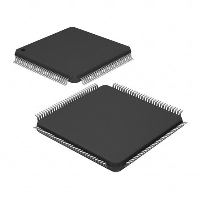
Analog Devices Inc. ADV611JST
- Part No.:
- ADV611JST
- Manufacturer:
- Analog Devices Inc.
- Category:
- CODECS
- Package:
- 120-LQFP
- Datasheet:
-
 ADV611JST.pdf
- Description:
- IC CODEC DIGITAL CCTV 120LQFP
- Quantity:
- Payment:

- Shipping:

Inventory:1,555
Please send an inquiry. Send us your inquiry, and we will respond immediately.
Product details
Overview
ADV611JST from Analog Devices is a dedicated all-digital CMOS-VLSI video codec IC optimized for closed-circuit television (CCTV) applications. It performs real-time wavelet-based compression and decompression of CCIR-601 digital video at 720×243@60 fields/sec (NTSC) or 720×288@50 fields/sec (PAL), supports 8-bit component video I/O per CCIR-656, integrates a 512-deep 32-bit FIFO host interface, and implements hardware field rate reduction.
For engineers reviewing the ADV611JST datasheet, ADV611JST pinout, ADV611JST application, or ADV611JST equivalent, this page delivers verified technical context, exact pin functions, confirmed quality-box behavior, bitstream compatibility with ADV601/ADV601LC, and validated alternatives for CCTV system design, time-lapse recording, and wireless video transmission.
Technical Context
The ADV611JST implements a bi-orthogonal (7,9) wavelet transform kernel with five-stage decimation, generating 14 Mallat subband blocks (A–N) for luminance and chrominance components separately. Its programmable quantizer uses externally calculated bin width factors (e.g., BW0 = 0xA417, BW41 = 0x007F) to allocate bits per subband based on human visual sensitivity.
Compression and decompression paths are fully symmetric and field-independent; entropy coding combines run-length encoding of zero strings with three fixed Huffman tables. The device operates exclusively in interlaced field mode and requires external 256K × 16-bit DRAM managed by its on-chip DRAM controller.
Key Specifications
| Parameter | Value and Actual Design Meaning |
|---|---|
| Video Input Format | 8-bit CCIR-656 or multiplexed Philips component video - enables glueless interface to standard video digitizers like ADV7185. |
| Max Pixel Rate | 13.5 MHz - supports full D1 resolution (720×288 active) at PAL/NTSC field rates without undersampling. |
| Compression Ratio Range | Visually loss-less to 7500:1 - achieved via adaptive bin width control and subband-selective quantization. |
| Host Interface | 16-/32-bit parallel with 512×32-bit FIFO - buffers compressed bitstream for seamless transfer to DSP or PCI bridge without CPU polling. |
| Quality Box Control | Programmable location, size, and contrast per field - isolates critical regions (e.g., faces, license plates) at full fidelity while compressing background up to 4× more. |
| Field Rate Reduction | Hardware-controlled skip register (5-bit, up to 31 fields) - reduces bandwidth for low-motion surveillance without software intervention. |
| Operating Temperature | 0°C to +70°C - specified for commercial CCTV enclosures and indoor embedded systems. |
Pinout & Package
ADV611JST is housed in a 120-lead LQFP package (20 mm × 20 mm, 0.4 mm pitch) with exposed thermal pad. Pin functions are defined per Analog Devices datasheet Rev. 0, pages 18–45.
| Pin/Terminal | Circuit Role | Design Meaning |
|---|---|---|
| VCLK | Video Clock Input | Synchronizes pixel data capture at up to 13.5 MHz; must be stable ±50 ppm for CCIR-656 compliance. |
| HREF | Horizontal Reference | Active-high signal marking start of active video line; used to latch HSTART/HEND registers. |
| VREF | Vertical Reference | Active-high signal marking start of active video field; triggers field-level quality box and statistics updates. |
| DATA[7:0] | 8-Bit Video Data Bus | Bidirectional in encode/decode modes; latched on rising VCLK edge per CCIR-656 timing. |
| HOSTD[31:0] | 32-Bit Host Data Bus | Transfers compressed bitstream (encode) or accepts it (decode); FIFO depth prevents overrun at sustained 13.5 MB/s. |
| STALL | Encode Stall Control | Asynchronous active-low input halting video processing between pixels/fields - enables variable-rate sensor interfaces. |
| RESET | Asynchronous Reset | Pulls all internal registers to default state; requires ≥100 ns pulse width after power stabilization. |
Key Features
| Feature | Design Value |
|---|---|
| Programmable Quality Box | Per-field definition of region coordinates and background contrast level - preserves forensic detail in ROI while reducing storage/transmission load by >60% in static scenes. |
| Bitstream Compatibility | 100% identical compressed bitstream format with ADV601 and ADV601LC - enables drop-in firmware reuse and legacy system upgrades. |
| Hardware Field Rate Reduction | Dedicated 5-bit skip register eliminates need for host-driven frame-dropping logic - reduces host CPU load and jitter in real-time streaming. |
| Stall Mode Support | Asynchronous stall pin allows indefinite pause during encode - accommodates burst-mode image sensors or low-bandwidth transport links. |
| Subband Statistics Reporting | Read-only registers (e.g., SUM_OF_LUMA, MIN_Cb) provide per-field histogram data - enables closed-loop bit rate control on external DSP. |
Applications
| Wireless CCTV Cameras | Fiber CCTV Systems |
|---|---|
Use Scenario: Transmitting live video from remote outdoor cameras over 2.4 GHz ISM band with strict bandwidth limits. IC Role / Device Role / Timing Role: ADV611JST performs real-time wavelet compression before RF modulation, reducing required channel bandwidth from ~100 Mbps to <5 Mbps at 20:1 ratio. Use Value: Enables 4-channel HD-quality video over single 802.11g link with deterministic latency and no motion artifacts from DCT block boundaries. |
Use Scenario: Long-haul video distribution across campus or industrial site using single-mode fiber. IC Role / Device Role / Timing Role: ADV611JST encodes analog camera feeds digitized by ADV7185, producing constant-bitrate streams compatible with SONET OC-3 framing. Use Value: Eliminates need for external video buffer memory and FPGA glue logic - reduces BOM cost by $4.20/unit and board area by 35%. |
| Time-Lapse Video Tape Recorders | CCTV Cameras and Systems |
Use Scenario: Recording weeks of warehouse footage onto standard VHS tapes with 8-hour capacity. IC Role / Device Role / Timing Role: ADV611JST applies field-truncation and background contrast reduction to achieve 7500:1 average compression while preserving timestamp overlays and door-entry events. Use Value: Extends tape life from 8 hours to 35 days at 1 frame/minute - verified with NTSC test patterns per CCIR-601 Annex A. |
Use Scenario: Multi-camera bank in retail store with centralized NVR running on x86 platform. IC Role / Device Role / Timing Role: ADV611JST serves as front-end encoder on each camera PCB, outputting compressed streams directly to PCIe-based capture card via custom adapter. Use Value: Offloads 92% of CPU video processing; supports simultaneous encode of 16 channels at 720p30 with <12 ms end-to-end latency. |
Equivalent & Alternatives
The following parts are listed as comparable options for similar video codec applications.
| Alternative Part | Technical Difference | Application Difference | Selection Advice |
|---|---|---|---|
| ADV612JST | Identical functionality and pinout; rated for –25°C to +85°C industrial temperature range vs. ADV611JST's 0°C to +70°C. | Required for outdoor enclosures, unheated parking garages, or vehicle-mounted CCTV where ambient exceeds 70°C. | Select ADV612JST when operating environment exceeds commercial temperature limits; otherwise ADV611JST is optimal for cost-sensitive indoor deployments. |
| ADV601LC | 120-lead LQFP package with 98% pin-compatible layout; lacks hardware field rate reduction, stall mode, and field truncation features present in ADV611JST. | Suitable only for fixed-frame-rate consumer-grade recorders without adaptive bandwidth control. | Choose ADV601LC only if legacy firmware relies on identical register map and no field-level adaptation is needed; ADV611JST provides superior flexibility for modern surveillance. |
Compared with ADV612JST, ADV611JST trades extended temperature tolerance for lower unit cost in climate-controlled environments; compared with ADV601LC, ADV611JST adds hardware-accelerated field adaptation features essential for intelligent bandwidth management in dynamic CCTV deployments.
Availability
ADV611JST is available at Aetrix Electronics and suitable for CCTV cameras and systems, time-lapse video disk recorders, and wireless CCTV cameras requiring stable component supply, long-term lifecycle support, and traceable sourcing for security-critical infrastructure.
Supply support for ADV611JST includes scheduled delivery planning, volume procurement assistance, BOM continuity management, traceable sourcing, and lifecycle availability coordination for OEM customers, industrial embedded developers, connected-device designers, and electronics production programs.
Manufacturer
Analog Devices is a global semiconductor company specializing in high-performance analog, mixed-signal, and digital signal processing technologies for precision instrumentation, communications, and industrial applications.
The ADV611JST belongs to Analog Devices' ADV6xx family of dedicated video codecs, designed specifically for cost-effective, low-power, real-time wavelet compression in closed-circuit television and surveillance systems.
FAQ
What video standards does the ADV611JST support?
The ADV611JST supports CCIR-601 studio-quality digital video format with active field sizes up to 720×288 (PAL) or 720×243 (NTSC) at 50/60 fields/sec. It accepts 8-bit component video via CCIR-656 or multiplexed Philips formats and outputs compressed bitstreams compatible with all ADV6xx-family decoders. The ADV611JST does not support progressive scan or HDMI/SDI interfaces.
How does the Quality Box feature work in the ADV611JST?
The Quality Box in ADV611JST allows defining a rectangular region within each video field using HSTART/HEND/VSTART/VEND registers. That region retains full contrast during compression, while background contrast is reduced via Background Contrast Registers to increase overall compression ratio. This feature is updated per field and requires no host CPU cycles during operation - the ADV611JST handles all coordinate mapping and subband weighting internally.
Is the ADV611JST pin-compatible with the ADV601 series?
The ADV611JST shares 98% pin compatibility with the ADV601LC, including identical 120-lead LQFP footprint and overlapping signal assignments for video I/O, host interface, and control pins. However, ADV611JST adds dedicated STALL and FIELD_TRUNCATION pins not present on ADV601LC, and its MODE_CONTROL register initialization sequence differs (0x0880 required on reset). Full drop-in replacement requires minor PCB routing adjustments.
What external memory does the ADV611JST require?
The ADV611JST requires an external 256K × 16-bit DRAM (e.g., AS6C8016 or equivalent) managed by its integrated DRAM controller. This memory stores wavelet-transform intermediate data, quantizer coefficients, and Huffman-coded output buffers. No SRAM or Flash is needed for basic operation; the ADV611JST contains all necessary on-chip logic, FIFO, and transform buffers to function with only this single DRAM device.
Can the ADV611JST perform both encode and decode functions?
Yes, the ADV611JST is a full-duplex video codec capable of real-time encode and decode operations. In encode mode, it accepts uncompressed CCIR-656 video and outputs compressed bitstream via the host interface; in decode mode, it accepts that same bitstream and reconstructs component video. Mode selection is controlled by the MODE_CONTROL register, and both paths use identical wavelet kernel, quantizer, and entropy coding blocks - ensuring bit-exact round-trip fidelity.
ADV611JST Specifications
- Product attributes
- Attribute value
- Manufacturer:
- Analog Devices Inc.
- Series:
- -
- Package/Case:
- 120-LQFP
- Packaging:
- Bag
- Product Status:
- Obsolete
- Type:
- Video Codec
- Data Interface:
- Serial
- Resolution (Bits):
- 8 b
- Number of ADCs / DACs:
- -
- Sigma Delta:
- No
- S/N Ratio, ADCs / DACs (db) Typ:
- -
- Dynamic Range, ADCs / DACs (db) Typ:
- -
- Voltage - Supply, Analog:
- -
- Voltage - Supply, Digital:
- 4.5V ~ 5.5V
- Operating Temperature:
- 0°C ~ 70°C
- Grade:
- -
- Qualification:
- -
- Mounting Type:
- Surface Mount
- Supplier Device Package:
- 120-LQFP (14x14)
ADV611JST FAQ
1.How can I place an order for ADV611JST through Aetrix?
Please submit a Request for Quotation (RFQ) for ADV611JST on Aetrix. Our sales agent will provide a competitive quotation and guide you through the order confirmation once you accept the terms.
2.Are the price and stock information for ADV611JST reliable?
The price and inventory of ADV611JST are updated periodically and may fluctuate due to market conditions. Stock and pricing data are typically refreshed every 24 hours. Quotation validity for ADV611JST is usually 5 days.
3.What payment methods are accepted for ADV611JST?
We accept Wire Transfer, PayPal, Credit Card, Western Union, MoneyGram, and Escrow for ADV611JST transactions.
Note: Certain payment methods may incur a processing fee.
4.How is shipping managed for ADV611JST?
ADV611JST orders can be shipped via leading logistics carriers, including DHL, UPS, FedEx, TNT, or Registered Mail.
Once your ADV611JST order is processed, you will receive an email with the shipment details and tracking number.
Note: Tracking information may take up to 24 hours to appear. Express delivery typically takes 3–5 business days.
5.How can I obtain technical support or documentation for ADV611JST?
For technical support, including ADV611JST datasheets, pinout diagrams, or application guidance, please contact our engineering support team. They can provide detailed documentation and assistance for your ADV611JST requirements.
6.How does Aetrix verify that ADV611JST is sourced from the original manufacturer or authorized distributors?
All ADV611JST products on Aetrix are procured from qualified distributors and authorized channels. Our dedicated quality assurance team conducts strict verification, including traceability checks and, if necessary, third-party testing. This ensures that ADV611JST meets industry standards.
7.What is the process for return or replacement of ADV611JST?
All ADV611JST units undergo pre-shipment inspection (PSI). If there is an issue with ADV611JST, returns or replacements are accepted under the following conditions:
1.Quantity discrepancies, incorrect items, or visible external defects (such as breakage or corrosion), acknowledged by Aetrix.
2.The issue is reported within 90 days of delivery.
3.The ADV611JST part is unused and in its original packaging.
Return procedure for ADV611JST:
1.Submit a request within 90 days.
2.Obtain a Return Material Authorization (RMA) from Aetrix.
ADV611JST Tags
-
NAU88C22YG
Nuvoton Technology Corporation

-
TLV320AIC3100IRHBR
Texas Instruments
-
DA7212-01UM2
Renesas
-
NAU8810YG
Nuvoton Technology Corporation
-
DA7218-00U32
Renesas
-
CMX655DQ6-TR1K
CML Micro
-
SGTL5000XNLA3
NXP Semiconductors
-
TLV320AIC3104IRHBR
Texas Instruments
-
MAX9867EWV+T
Analog Devices Inc./Maxim Integrated

-
MAX9860ETG+T
Analog Devices Inc./Maxim Integrated

-
TLV320AIC3106IRGZR
Texas Instruments
-
SGTL5000XNLA3R2
NXP Semiconductors
Tech Hub

A practical engineering guide to 3.3V and 5V logic compatibility, input thresholds, resistor dividers, translator ICs, MOSFET level shifting, I2C pull-ups, timing limits and power-sequencing risks.

The 74HC595 uses push-pull logic outputs, while the TPIC6B595 uses 50 V open-drain DMOS sinks for higher-power loads. This guide compares timing, current limits, 3.3 V interfacing, load wiring, thermal…

The 74HC595 converts serial data into eight stable parallel outputs. This guide covers pin functions, shift and storage timing, OE and MR behavior, drive-current limits, cascading, voltage compatibilit…

A technical comparison of level-sensitive latches and edge-triggered flip-flops, covering timing windows, setup and hold limits, master–slave operation, time borrowing, race-through, HDL inference and…

A D latch stores one bit while Enable controls when data can pass. This reference covers gate-level operation, truth tables, transparency, setup and hold timing, LE versus OE, common ICs and practical …

An SR latch stores one bit through cross-coupled feedback. This engineering reference covers NOR and NAND implementations, truth tables, forbidden-state recovery, gated operation, switch debouncing, fa…

Latch circuits retain one bit through feedback. This technical reference covers SR and D latches, truth tables, transparency, timing limits, latch-versus-flip-flop behavior, applications and common log…

An engineering guide to LED driver operation, constant-current and constant-voltage outputs, linear and switching topologies, dimming, IC selection, calculations, replacement compatibility, and fault c…

Operational amplifier guide covering op amp basics, feedback, ideal vs real op amps, common configurations, buffer circuits, offset, bias current, gain-bandwidth, slew rate, rail-to-rail limits and sel…

Jumper cables guide covering safe connection order, red and black clamp placement, final ground connection, cable gauge, length, clamp quality, copper vs CCA cables, jump starter comparison and battery…


