
 My Inquiry
 My Account


Analog Devices Inc. ADV7120KN30
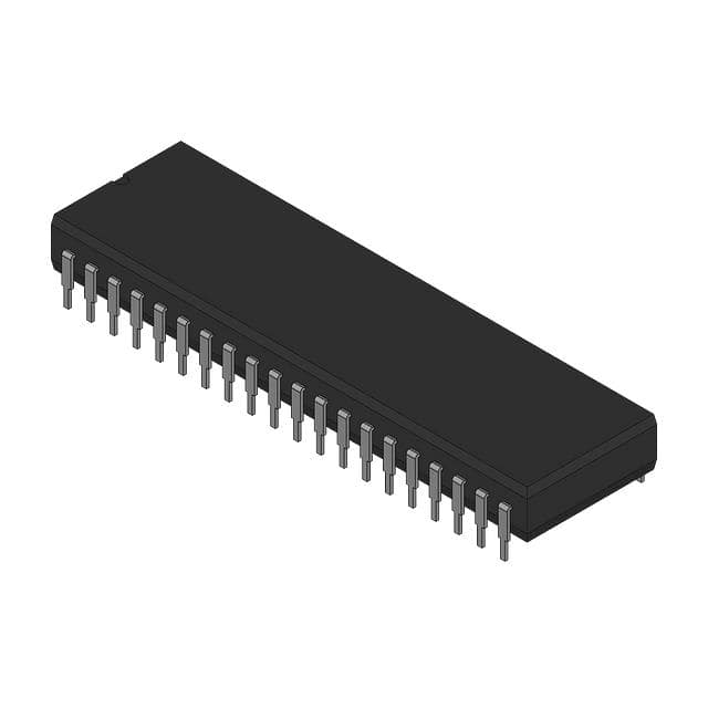
- Part No.:
- ADV7120KN30
- Manufacturer:
- Analog Devices Inc.
- Category:
- Digital to Analog Converters (DAC)
- Package:
- 40-DIP (0.600", 15.24mm)
- Datasheet:
-
 ADV7120KN30.pdf
- Description:
- IC DAC 8BIT A-OUT 40DIP
- Quantity:
- Payment:

- Shipping:

Inventory:6,331
Please send an inquiry. Send us your inquiry, and we will respond immediately.
Product details
Overview
ADV7120KN30 from Analog Devices is a CMOS triple 8-bit video DAC engineered for high-resolution color graphics and video systems operating at up to 30 MHz pixel clock rate. It integrates three matched current-output DACs (IOR, IOG, IOB), TTL-compatible digital inputs, and RS-343A/RS-170-compliant analog outputs-enabling direct drive of doubly terminated 75 Ω coaxial video loads without external buffering. It supports composite sync, blank, and reference white control for CRT and RGB monitor interfaces.
For engineers reviewing the ADV7120KN30 datasheet, ADV7120KN30 pinout, ADV7120KN30 application, or ADV7120KN30 equivalent, key selection considerations include its 30 MHz speed grade, 40-pin plastic DIP (N-40A) package, guaranteed monotonicity (±0.5 LSB DNL), 8-bit resolution, and compatibility with standard video timing and termination schemes used in CAE/CAD, instrumentation, and desktop publishing systems.
Technical Context
The ADV7120KN30 implements a segmented current-steering DAC architecture with monolithic CMOS integration, ensuring tight DAC-to-DAC matching (≤5% max) and low glitch impulse (50 pV·s typ). Its digital interface latches 24-bit RGB pixel data (R0–R7, G0–G7, B0–B7) and control signals (SYNC, BLANK, REF WHITE) on the rising edge of the CLOCK input.
It features an internal reference amplifier with external VREF (1.14–1.26 V) and FS ADJUST pin for full-scale current calibration via RSET resistor. Analog outputs operate as high-impedance current sources (IOR/IOG/IOB: 15–22 mA range; ISYNC: programmable sync current), with output compliance from –1 V to +1.4 V and typical output impedance of 100 kΩ.
Key Specifications
| Parameter | Value and Actual Design Meaning |
|---|---|
| Max Clock Rate | 30 MHz - defines maximum pixel data throughput for noninterlaced 640×480@60 Hz or interlaced 1024×768@30 Hz video systems |
| Resolution | 8 bits per channel - delivers 256 discrete gray levels per RGB channel, supporting standard RS-343A video amplitude steps |
| Differential Nonlinearity | ±0.5 LSB max - guarantees monotonic transfer function critical for artifact-free video ramp generation |
| Integral Nonlinearity | ±1 LSB max - ensures end-point accuracy within one least-significant step across full 0–255 code range |
| Gray Scale Current Range | 15–22 mA - sets full-scale analog output magnitude; calibrated via RSET to meet RS-343A white level (19.05 mA typ) |
| Power Supply | +5 V ±5% - single-supply operation compatible with standard TTL logic rails and industrial 5 V power domains |
| Analog Output Skew | 2 ns max - maintains sub-pixel timing alignment between RGB channels for color fidelity in high-speed video |
Pinout & Package
ADV7120KN30 is housed in a 40-pin plastic DIP (N-40A) package with 0.6-inch width. Pin assignments follow standard Analog Devices video DAC layout optimized for signal integrity and thermal dissipation in analog-video PCB designs.
| Pin/Terminal | Circuit Role | Design Meaning |
|---|---|---|
| R0–R7, G0–G7, B0–B7 | Parallel TTL pixel data inputs | Latched on CLOCK rising edge; R0/G0/B0 = LSB; unused bits tied to GND/VAA per layout guidelines |
| CLOCK | Pixel clock input | TTL-compatible; rising edge triggers simultaneous latch of all 24-bit RGB data and control inputs |
| BLANK, SYNC, REF WHITE | Video control inputs | TTL-level; BLANK forces outputs to blanking level (7.62 mA on IOG); REF WHITE overrides data to white level (26.67 mA) |
| IOR, IOG, IOB | Current-output video channels | High-Z current sources; each drives 37.5 Ω load (doubly terminated 75 Ω cable); IOG also carries ISYNC when connected |
| ISYNC | Sync current output | Programmable current source (3.455 × VREF/RSET mA); typically wired to IOG to embed sync on green channel |
| FS ADJUST | Full-scale calibration node | Connect RSET (560 Ω typical) to GND to set IOG = 26.67 mA and IOR/IOB = 19.05 mA per RS-343A |
| VREF | Reference voltage input | Accepts 1.14–1.26 V external reference (e.g., AD589); 0.1 µF ceramic cap required to VAA at COMP pin |
| VAA, GND | Analog supply and ground | All VAA and GND pins must be connected; separate analog ground plane recommended with ferrite-bead isolation |
Key Features
| Feature | Design Value |
|---|---|
| Triple 8-bit DAC architecture | Enables simultaneous RGB video reconstruction with ≤2 ns inter-channel skew for accurate color registration |
| RS-343A/RS-170 compliance | Output current levels and timing meet broadcast video standards without external amplifiers or level-shifting circuitry |
| Monotonicity guarantee | ±0.5 LSB DNL ensures no missing codes in grayscale ramps-critical for medical imaging and test pattern generation |
| Integrated sync/blank control | Eliminates need for external logic to encode composite sync or blanking pulses onto analog outputs |
| Single +5 V supply operation | Reduces system BOM count and simplifies power delivery versus dual-supply video DAC alternatives |
Applications
| CAE/CAD Workstations | Instrumentation Displays |
|---|---|
Use Scenario: Real-time rendering of vector-based schematics and mechanical models on high-resolution RGB monitors. IC Role / Device Role / Timing Role: ADV7120KN30 converts FPGA- or GPU-generated pixel data into synchronized analog RGB signals at 30 MHz dot clock. Use Value: Delivers artifact-free grayscale ramps and precise color boundaries essential for CAD layer visibility and measurement accuracy. | Use Scenario: Driving analog oscilloscope or spectrum analyzer front-panel displays with calibrated intensity and timing. IC Role / Device Role / Timing Role: ADV7120KN30 acts as waveform reconstruction engine, converting digitized acquisition data into analog video output with <2 ns RGB skew. Use Value: Enables sub-nanosecond timing correlation between displayed waveforms and trigger events due to deterministic DAC latency. |
| Desktop Publishing Systems | Image Processing Terminals |
Use Scenario: Generating high-fidelity RGB output for prepress proofing and color-critical page layout previews. IC Role / Device Role / Timing Role: ADV7120KN30 serves as final-stage video DAC in RIP (Raster Image Processor) pipelines, accepting parallel pixel streams from frame buffers. Use Value: ±1 LSB INL ensures consistent tone reproduction across 256 gray levels-vital for halftone screening and spot-color verification. | Use Scenario: Real-time display of processed medical or satellite imagery requiring faithful luminance mapping. IC Role / Device Role / Timing Role: ADV7120KN30 reconstructs 8-bit monochrome or pseudocolor video frames from DSP co-processors at up to 30 MHz pixel rate. Use Value: Guaranteed monotonicity prevents false contours in low-contrast regions, preserving diagnostic detail in X-ray or MRI visualization. |
Equivalent & Alternatives
The following parts are listed as comparable options for similar triple 8-bit video DAC applications.
| Alternative Part | Technical Difference | Application Difference | Selection Advice |
|---|---|---|---|
| ADV7123KST30 | 48-lead TQFP package; REF WHITE and ISYNC pins omitted; same 30 MHz speed grade and electrical specs | Suitable for space-constrained PCBs where DIP footprint is unacceptable; requires layout revision for pinout and decoupling | Select when board area is limited and surface-mount assembly is preferred over through-hole DIP. |
| THS8135PAP | 30 MHz triple 8-bit DAC from Texas Instruments; different pinout; requires external reference; ±1 LSB INL but no guaranteed monotonicity spec | Compatible with RS-343A loads but lacks integrated sync/blank logic-requires external gate array for control encoding | Choose only if existing design uses TI ecosystem and external sync logic is already present. |
Compared with ADV7120KN30, ADV7123KST30 offers identical video performance in a smaller footprint but removes two control pins, while THS8135PAP provides similar speed and resolution but shifts system-level complexity to external components for video control functions.
Availability
ADV7120KN30 is available at Aetrix Electronics and suitable for CAE/CAD workstations, instrumentation displays, desktop publishing systems, and image processing terminals requiring stable component supply across extended production lifecycles.
Supply support for ADV7120KN30 includes scheduled delivery planning, volume procurement assistance, BOM continuity management, traceable sourcing, and lifecycle availability coordination for OEM customers, industrial embedded developers, connected-device designers, and electronics production programs.
Manufacturer
Analog Devices, Inc. is a global leader in high-performance analog, mixed-signal, and digital signal processing semiconductors, headquartered in Norwood, MA.
The ADV7120 product line was designed specifically for high-resolution video signal reconstruction in graphics, instrumentation, and broadcast equipment-emphasizing timing precision, DAC matching, and direct RS-343A/RS-170 compliance.
FAQ
What is the maximum pixel clock frequency supported by the ADV7120KN30?
The ADV7120KN30 is rated for a maximum clock frequency of 30 MHz, as specified in the Ordering Guide and Timing Characteristics table. This speed grade supports common video formats including 640×480@60 Hz noninterlaced and 1024×768@30 Hz interlaced. Exceeding 30 MHz may result in timing violations, increased DNL, or loss of monotonicity. The ADV7120KN30 datasheet confirms t3 (clock cycle time) ≥33.3 ns for this variant, directly corresponding to 30 MHz operation.
Does the ADV7120KN30 require an external voltage reference, and what is the acceptable range?
Yes, the ADV7120KN30 requires an external voltage reference applied to the VREF pin. The specified range is 1.14 V to 1.26 V, with optimal performance achieved at 1.235 V (e.g., using the AD589 voltage reference). The reference must be stable and low-noise; the datasheet explicitly warns against using resistor divider networks. A 0.1 µF ceramic capacitor is mandatory between VREF and VAA for decoupling, and a 0.1 µF capacitor is required between COMP and VAA for amplifier compensation.
How is full-scale output current calibrated on the ADV7120KN30?
Full-scale output current on the ADV7120KN30 is calibrated using an external resistor (RSET) connected between the FS ADJUST pin and GND. For the green channel (IOG), IOG (mA) = 12,082 × VREF (V) / RSET (Ω); for red and blue (IOR/IOB), the relationship is IOR/IOB (mA) = 8,628 × VREF (V) / RSET (Ω). With VREF = 1.235 V and RSET = 560 Ω, IOG = 26.67 mA and IOR/IOB = 19.05 mA-matching RS-343A white and black level specifications.
Can the ADV7120KN30 drive standard 75 Ω video monitors directly?
Yes, the ADV7120KN30 can drive standard 75 Ω video monitors directly when configured with proper termination. Each current output (IOR, IOG, IOB) is a high-impedance source capable of driving a 37.5 Ω source termination into a 75 Ω load (doubly terminated coaxial cable), generating RS-343A-compliant voltage levels. No external buffer is required for short cable runs (<10 m). For longer cables or RS-170 compliance, source termination resistance is increased to 150 Ω per channel.
What is the purpose of the ISYNC pin on the ADV7120KN30, and how is it used?
The ISYNC pin on the ADV7120KN30 is a programmable current output used to embed composite sync information onto the green video channel. When the SYNC input is high, ISYNC sources current equal to 3.455 × VREF / RSET mA. It is typically connected directly to the IOG pin so that sync pulses appear superimposed on the green analog waveform. If sync encoding is not needed, SYNC should be held low and ISYNC tied to AGND to prevent interference with the green channel output.
ADV7120KN30 Specifications
- Product attributes
- Attribute value
- Manufacturer:
- Analog Devices Inc.
- Series:
- -
- Package/Case:
- 40-DIP (0.600", 15.24mm)
- Packaging:
- Bulk
- Product Status:
- Active
- Programmable:
- Not Verified
- Number of Bits:
- 8
- Number of D/A Converters:
- 3
- Settling Time:
- -
- Output Type:
- Current - Unbuffered
- Differential Output:
- No
- Data Interface:
- Parallel
- Reference Type:
- External
- Voltage - Supply, Analog:
- 4.75V ~ 5.25V
- Voltage - Supply, Digital:
- 4.75V ~ 5.25V
- INL/DNL (LSB):
- ±1 (Max), ±0.5 (Max)
- Architecture:
- Current Source
- Operating Temperature:
- 0°C ~ 70°C
- Supplier Device Package:
- 40-PDIP
- Mounting Type:
- Through Hole
- Grade:
- -
- Qualification:
- -
ADV7120KN30 FAQ
1.How can I place an order for ADV7120KN30 through Aetrix?
Please submit a Request for Quotation (RFQ) for ADV7120KN30 on Aetrix. Our sales agent will provide a competitive quotation and guide you through the order confirmation once you accept the terms.
2.Are the price and stock information for ADV7120KN30 reliable?
The price and inventory of ADV7120KN30 are updated periodically and may fluctuate due to market conditions. Stock and pricing data are typically refreshed every 24 hours. Quotation validity for ADV7120KN30 is usually 5 days.
3.What payment methods are accepted for ADV7120KN30?
We accept Wire Transfer, PayPal, Credit Card, Western Union, MoneyGram, and Escrow for ADV7120KN30 transactions.
Note: Certain payment methods may incur a processing fee.
4.How is shipping managed for ADV7120KN30?
ADV7120KN30 orders can be shipped via leading logistics carriers, including DHL, UPS, FedEx, TNT, or Registered Mail.
Once your ADV7120KN30 order is processed, you will receive an email with the shipment details and tracking number.
Note: Tracking information may take up to 24 hours to appear. Express delivery typically takes 3–5 business days.
5.How can I obtain technical support or documentation for ADV7120KN30?
For technical support, including ADV7120KN30 datasheets, pinout diagrams, or application guidance, please contact our engineering support team. They can provide detailed documentation and assistance for your ADV7120KN30 requirements.
6.How does Aetrix verify that ADV7120KN30 is sourced from the original manufacturer or authorized distributors?
All ADV7120KN30 products on Aetrix are procured from qualified distributors and authorized channels. Our dedicated quality assurance team conducts strict verification, including traceability checks and, if necessary, third-party testing. This ensures that ADV7120KN30 meets industry standards.
7.What is the process for return or replacement of ADV7120KN30?
All ADV7120KN30 units undergo pre-shipment inspection (PSI). If there is an issue with ADV7120KN30, returns or replacements are accepted under the following conditions:
1.Quantity discrepancies, incorrect items, or visible external defects (such as breakage or corrosion), acknowledged by Aetrix.
2.The issue is reported within 90 days of delivery.
3.The ADV7120KN30 part is unused and in its original packaging.
Return procedure for ADV7120KN30:
1.Submit a request within 90 days.
2.Obtain a Return Material Authorization (RMA) from Aetrix.
ADV7120KN30 Tags
-
MCP47A1T-A0E/LT
Microchip Technology

-
MCP4706A0T-E/CH
Microchip Technology
-
MCP4716A0T-E/MAY
Microchip Technology
-
MCP4716A0T-E/CH
Microchip Technology
-
MCP4726A0T-E/CH
Microchip Technology
-
MCP4725A0T-E/CH
Microchip Technology
-
MCP4725A1T-E/CH
Microchip Technology
-
MCP4725A2T-E/CH
Microchip Technology
-
MCP4726A1T-E/CH
Microchip Technology
-
MCP4726A3T-E/CH
Microchip Technology
-
MCP4726A2T-E/CH
Microchip Technology
-
MCP4726A0T-E/MAY
Microchip Technology
Tech Hub

A practical engineering guide to 3.3V and 5V logic compatibility, input thresholds, resistor dividers, translator ICs, MOSFET level shifting, I2C pull-ups, timing limits and power-sequencing risks.

The 74HC595 uses push-pull logic outputs, while the TPIC6B595 uses 50 V open-drain DMOS sinks for higher-power loads. This guide compares timing, current limits, 3.3 V interfacing, load wiring, thermal…

The 74HC595 converts serial data into eight stable parallel outputs. This guide covers pin functions, shift and storage timing, OE and MR behavior, drive-current limits, cascading, voltage compatibilit…

A technical comparison of level-sensitive latches and edge-triggered flip-flops, covering timing windows, setup and hold limits, master–slave operation, time borrowing, race-through, HDL inference and…

A D latch stores one bit while Enable controls when data can pass. This reference covers gate-level operation, truth tables, transparency, setup and hold timing, LE versus OE, common ICs and practical …

An SR latch stores one bit through cross-coupled feedback. This engineering reference covers NOR and NAND implementations, truth tables, forbidden-state recovery, gated operation, switch debouncing, fa…

Latch circuits retain one bit through feedback. This technical reference covers SR and D latches, truth tables, transparency, timing limits, latch-versus-flip-flop behavior, applications and common log…

An engineering guide to LED driver operation, constant-current and constant-voltage outputs, linear and switching topologies, dimming, IC selection, calculations, replacement compatibility, and fault c…

Operational amplifier guide covering op amp basics, feedback, ideal vs real op amps, common configurations, buffer circuits, offset, bias current, gain-bandwidth, slew rate, rail-to-rail limits and sel…

Jumper cables guide covering safe connection order, red and black clamp placement, final ground connection, cable gauge, length, clamp quality, copper vs CCA cables, jump starter comparison and battery…


