
 My Inquiry
 My Account


Analog Devices Inc. ADV7150LS85
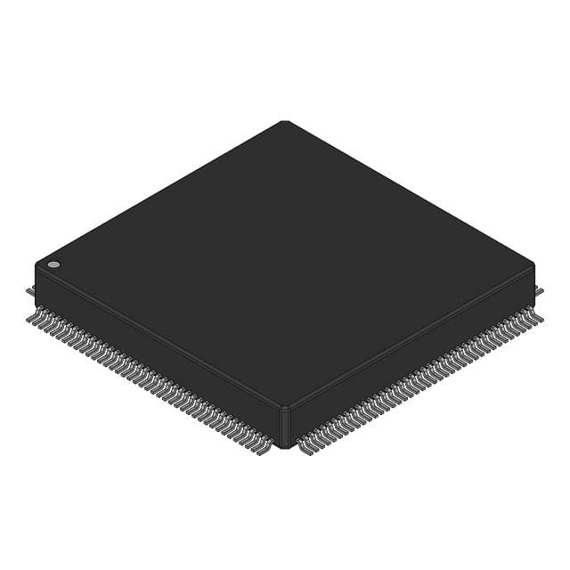
- Part No.:
- ADV7150LS85
- Manufacturer:
- Analog Devices Inc.
- Category:
- Digital to Analog Converters (DAC)
- Package:
- 160-BQFP
- Datasheet:
-
 ADV7150LS85.pdf
- Description:
- IC DAC 10BIT A-OUT 160MQFP
- Quantity:
- Payment:

- Shipping:

Inventory:4,043
Please send an inquiry. Send us your inquiry, and we will respond immediately.
Product details
Overview
ADV7150LS85 from Analog Devices is a 160-pin QFP CMOS triple 10-bit video RAM-DAC optimized for 85 MHz true-color graphics output. It integrates 256×10 palette RAM per channel, gamma-corrected DACs, and programmable pixel port modes (24-/15-/8-bit), delivering RS-170/RS-343A-compatible analog RGB outputs with 17.22 µA LSB size and ±1 LSB INL. It serves in professional color prepress imaging systems requiring stable 85 MHz pixel clock operation and precise grayscale fidelity.
For engineers reviewing the ADV7150LS85 datasheet, ADV7150LS85 pinout, ADV7150LS85 application, or ADV7150LS85 equivalent, this page provides verified timing specs (t1 = 11.77 ns min cycle time), analog output compliance (0/+1.4 V), power draw (315 mA max at 85 MHz), and MPU interface timing (t21 = 45 ns CE low time) critical for frame buffer integration and video signal integrity validation.
Technical Context
The ADV7150LS85 implements a 30-bit gamma-corrected color pipeline: 24-bit input data indexes into three 256×10 palette RAMs, whose outputs drive triple 10-bit DACs with matched full-scale current (±3% DAC-to-DAC matching). Its pixel port supports 4:1, 2:1, or 1:1 multiplexing-enabling direct connection to four VRAM banks at 21.25 MHz each to achieve 85 MHz effective throughput.
On-chip clock control includes ECL-compatible differential CLOCK/CLOCK inputs, LOADOUT (fCLOCK/4), PRGCKOUT (programmable ÷4/÷8/÷16/÷32), and SCKOUT synchronized to BLANK. The MPU port uses 10-bit bidirectional D0–D9 with CE/R/W/C0/C1 addressing, supporting palette programming and register configuration without external glue logic.
Key Specifications
| Parameter | Value and Actual Design Meaning |
|---|---|
| Max Pixel Clock | 85 MHz - defines maximum real-time RGB video update rate for 8-bit pseudo or 15-bit true color modes |
| DAC Resolution | 10 bits - delivers 1,024 intensity levels per RGB channel with ±1 LSB integral nonlinearity |
| Gray Scale Error | ±5% - ensures consistent luminance response across full 0–100% IRE range in calibrated displays |
| Analog Output Current | 15–22 mA - drives doubly terminated 75 Ω RS-170 loads directly without external amplification |
| Power Supply | +5 V ±5% - requires single-supply rail with 315 mA max draw at 85 MHz operation |
| Operating Temperature | 0°C to +70°C - validated for commercial-grade graphics workstation environments |
| Output Skew | 2 ns max - maintains RGB signal alignment critical for color fidelity in high-resolution raster scanning |
Pinout & Package
Package: 160-lead plastic quad flatpack (QFP) with thermally enhanced copper heatslug (θJC < 1.08°C/W).
| Pin/Terminal | Circuit Role | Design Meaning |
|---|---|---|
| IOR, IOG, IOB | RGB Analog Current Outputs | High-impedance current sources driving RS-170/RS-343A video levels into 75 Ω loads; IOG also carries SYNC level when CR22 enabled |
| CLOCK, CLOCK | Differential ECL Clock Inputs | Accept ECL-level signals (VAA–0.8 V to VAA–1.8 V) for noise-immune 85 MHz pixel clock distribution |
| LOADIN | Pixel Data Latch Input | TTL-compatible rising-edge trigger that captures multiplexed R/G/B/PS0/PS1/BLANK/SYNC data into internal pipeline |
| PRGCKOUT | Programmable Clock Output | Divided pixel clock (÷4/÷8/÷16/÷32) used for synchronous timing of external frame buffers or shift registers |
| D0–D9 | MPU Bidirectional Data Bus | 10-bit interface for reading/writing palette RAM, command registers (CR1–CR3), and test registers (MR1) |
| VREF, RSET | Analog Reference & Full-Scale Trim | VREF = 1.235 V reference sets DAC accuracy; RSET resistor (280 Ω typical) calibrates absolute output current amplitude |
Key Features
| Feature | Design Value |
|---|---|
| Triple 10-bit gamma-corrected DACs | Enables 30-bit effective color depth with linearized luminance response for accurate grayscale reproduction |
| 256 × 10 palette RAM per channel | Allows dynamic color mapping and palette switching per scan line without CPU intervention |
| 4:1/2:1/1:1 pixel port multiplexing | Supports direct interface to up to four parallel VRAM banks, eliminating external serializer ICs |
| RS-170/RS-343A analog output compliance | Delivers broadcast-standard video levels (0–100 IRE) with no external buffering or level-shifting circuitry |
| On-chip clock divider & sync generator | Generates LOADOUT, PRGCKOUT, and SCKOUT from single ECL clock source-reducing system BOM count |
Applications
| Professional Color Prepress Imaging | High-Resolution Graphics Workstations |
|---|---|
Use Scenario: Digital proofing systems generating 300+ DPI CMYK separations from RGB source files. IC Role / Device Role / Timing Role: ADV7150LS85 converts processed RGB pixel data into calibrated analog video for CRT-based soft-proof monitors. Use Value: ±5% gray scale error and 10-bit DAC resolution ensure accurate tonal reproduction critical for press-ready color matching. |
Use Scenario: CAD/CAM terminals rendering complex vector graphics and shaded 3D models in real time. IC Role / Device Role / Timing Role: ADV7150LS85 acts as the final video output stage, accepting 85 MHz pixel data from dual-port VRAM and generating synchronized RGB analog outputs. Use Value: 4:1 multiplexing allows four 21.25 MHz VRAM banks to feed the device, sustaining full-screen 1280×1024@75 Hz refresh without bandwidth bottlenecks. |
| Medical Diagnostic Displays | Broadcast-Quality Video Test Equipment |
Use Scenario: DICOM-compliant grayscale monitors displaying MRI/CT scans where subtle contrast differences indicate pathology. IC Role / Device Role / Timing Role: ADV7150LS85 drives high-stability analog CRT or LCD back-end with precise 10-bit luminance control. Use Value: ±1 LSB differential nonlinearity and 17.22 µA LSB size enable discrimination of ≤0.1% intensity deltas across diagnostic grayscale windows. |
Use Scenario: Waveform monitors and vectorscopes validating NTSC/PAL signal integrity during production switcher calibration. IC Role / Device Role / Timing Role: ADV7150LS85 generates reference RGB test patterns (e.g., color bars, PLUGE) with RS-170 timing compliance. Use Value: Built-in SYNC/BLANK handling and 2 ns RGB skew guarantee accurate timing alignment required for waveform analysis accuracy. |
Equivalent & Alternatives
The following parts are listed as comparable options for similar video RAM-DAC applications.
| Alternative Part | Technical Difference | Application Difference | Selection Advice |
|---|---|---|---|
| ADV7150LS110 | Higher 110 MHz pixel clock rating; identical pinout, package, and register map | Supports higher-resolution modes (e.g., 1600×1200@60 Hz) not achievable with ADV7150LS85's 85 MHz limit | Select when system clock budget exceeds 85 MHz and board layout allows same 160-pin QFP footprint |
| ADV7151LS85 | Same 85 MHz speed grade but implements 24-bit "standard" (non-gamma-corrected) true color instead of gamma-corrected mode | Used in applications requiring linear RGB output (e.g., scientific imaging) rather than perceptually uniform grayscale | Choose for linear transfer function needs; requires palette RAM reprogramming and different VREF/RSET calibration |
Compared with ADV7150LS85, the ADV7150LS110 offers headroom for future resolution upgrades while maintaining drop-in compatibility, whereas ADV7151LS85 trades gamma correction for linear response-requiring firmware and calibration changes but enabling precise photometric measurement workflows.
Availability
ADV7150LS85 is available at Aetrix Electronics and suitable for professional color prepress imaging, high-resolution graphics workstations, and medical diagnostic display systems requiring stable component supply and long-term obsolescence management.
Supply support for ADV7150LS85 includes scheduled delivery planning, volume procurement assistance, BOM continuity management, traceable sourcing, and lifecycle availability coordination for OEM customers, industrial embedded developers, connected-device designers, and electronics production programs.
Manufacturer
Analog Devices, Inc. is a global leader in high-performance analog, mixed-signal, and digital signal processing semiconductors, founded in 1965 and headquartered in Wilmington, MA.
The ADV7150 belongs to Analog Devices' ADV® video processor family, designed specifically for high-bandwidth, low-latency RGB video conversion in professional graphics workstations and prepress systems demanding sub-percent grayscale accuracy.
FAQ
What is the maximum pixel clock frequency supported by the ADV7150LS85?
The ADV7150LS85 supports a maximum pixel clock frequency of 85 MHz, as confirmed in the Ordering Guide and Timing Characteristics table. This speed grade enables operation in 1280×1024@75 Hz and other high-resolution modes requiring precise 11.77 ns minimum clock cycle time (t1). Exceeding 85 MHz may cause timing violations in LOADIN setup/hold or pipeline delays, leading to pixel corruption or color misalignment in the ADV7150LS85 output.
How does the ADV7150LS85 implement gamma correction?
The ADV7150LS85 implements hardware gamma correction via its 256×10 palette RAM structure and triple 10-bit DAC architecture, achieving 30-bit effective resolution. Each 8-bit pixel value indexes into the palette, which holds pre-distorted 10-bit values that compensate for CRT phosphor nonlinearity. This is distinct from software gamma tables-the ADV7150LS85 applies correction in real time during DAC conversion without CPU overhead.
Can the ADV7150LS85 drive standard 75 Ω video loads directly?
Yes, the ADV7150LS85 analog outputs (IOR, IOG, IOB) are specified to drive doubly terminated 75 Ω loads compliant with RS-170 and RS-343A standards. With white level output current of 17.62–19.05 mA and output compliance of 0/+1.4 V, it delivers proper 1.0 Vpp sync-tip-to-white video levels without external amplifiers or impedance-matching networks-verified under RL = 37.5 Ω load conditions per datasheet.
What is the function of the RSET pin on the ADV7150LS85?
The RSET pin on the ADV7150LS85 sets the full-scale output current amplitude for all three DAC channels via an external resistor to analog ground. Using the formula RSET (Ω) = 5,723 × VREF(V)/IOG(mA) (for 0 IRE pedestal), a 280 Ω resistor with 1.235 V VREF yields ~17.62 mA on IOG and matched currents on IOR/IOB. This trims absolute video level accuracy and ensures DAC-to-DAC matching within ±3%, critical for color balance in the ADV7150LS85.
Does the ADV7150LS85 support multiple palette configurations?
Yes, the ADV7150LS85 supports dynamic palette selection via PS0 and PS1 inputs, which act as pixel-by-pixel palette priority selects. When PS0/PS1 match values programmed in Mode Register MR16–MR17, the device's palette RAM is enabled for that pixel; otherwise, outputs default to blank level. This allows multiple ADV7150LS85 devices to share a common pixel bus while independently controlling color mapping per region or window.
ADV7150LS85 Specifications
- Product attributes
- Attribute value
- Manufacturer:
- Analog Devices Inc.
- Series:
- ADV7150
- Package/Case:
- 160-BQFP
- Packaging:
- Bulk
- Product Status:
- Active
- Programmable:
- Not Verified
- Number of Bits:
- 10
- Number of D/A Converters:
- 3
- Settling Time:
- -
- Output Type:
- Current - Unbuffered
- Differential Output:
- Yes
- Data Interface:
- Parallel
- Reference Type:
- External
- Voltage - Supply, Analog:
- 4.75V ~ 5.25V
- Voltage - Supply, Digital:
- 4.75V ~ 5.25V
- INL/DNL (LSB):
- ±1 (Max), ±1 (Max)
- Architecture:
- -
- Operating Temperature:
- 0°C ~ 70°C
- Supplier Device Package:
- 160-MQFP (28x28)
- Mounting Type:
- Surface Mount
- Grade:
- -
- Qualification:
- -
ADV7150LS85 FAQ
1.How can I place an order for ADV7150LS85 through Aetrix?
Please submit a Request for Quotation (RFQ) for ADV7150LS85 on Aetrix. Our sales agent will provide a competitive quotation and guide you through the order confirmation once you accept the terms.
2.Are the price and stock information for ADV7150LS85 reliable?
The price and inventory of ADV7150LS85 are updated periodically and may fluctuate due to market conditions. Stock and pricing data are typically refreshed every 24 hours. Quotation validity for ADV7150LS85 is usually 5 days.
3.What payment methods are accepted for ADV7150LS85?
We accept Wire Transfer, PayPal, Credit Card, Western Union, MoneyGram, and Escrow for ADV7150LS85 transactions.
Note: Certain payment methods may incur a processing fee.
4.How is shipping managed for ADV7150LS85?
ADV7150LS85 orders can be shipped via leading logistics carriers, including DHL, UPS, FedEx, TNT, or Registered Mail.
Once your ADV7150LS85 order is processed, you will receive an email with the shipment details and tracking number.
Note: Tracking information may take up to 24 hours to appear. Express delivery typically takes 3–5 business days.
5.How can I obtain technical support or documentation for ADV7150LS85?
For technical support, including ADV7150LS85 datasheets, pinout diagrams, or application guidance, please contact our engineering support team. They can provide detailed documentation and assistance for your ADV7150LS85 requirements.
6.How does Aetrix verify that ADV7150LS85 is sourced from the original manufacturer or authorized distributors?
All ADV7150LS85 products on Aetrix are procured from qualified distributors and authorized channels. Our dedicated quality assurance team conducts strict verification, including traceability checks and, if necessary, third-party testing. This ensures that ADV7150LS85 meets industry standards.
7.What is the process for return or replacement of ADV7150LS85?
All ADV7150LS85 units undergo pre-shipment inspection (PSI). If there is an issue with ADV7150LS85, returns or replacements are accepted under the following conditions:
1.Quantity discrepancies, incorrect items, or visible external defects (such as breakage or corrosion), acknowledged by Aetrix.
2.The issue is reported within 90 days of delivery.
3.The ADV7150LS85 part is unused and in its original packaging.
Return procedure for ADV7150LS85:
1.Submit a request within 90 days.
2.Obtain a Return Material Authorization (RMA) from Aetrix.
ADV7150LS85 Tags
-
MCP47A1T-A0E/LT
Microchip Technology

-
MCP4706A0T-E/CH
Microchip Technology
-
MCP4716A0T-E/MAY
Microchip Technology
-
MCP4716A0T-E/CH
Microchip Technology
-
MCP4726A0T-E/CH
Microchip Technology
-
MCP4725A0T-E/CH
Microchip Technology
-
MCP4725A1T-E/CH
Microchip Technology
-
MCP4725A2T-E/CH
Microchip Technology
-
MCP4726A1T-E/CH
Microchip Technology
-
MCP4726A3T-E/CH
Microchip Technology
-
MCP4726A2T-E/CH
Microchip Technology
-
MCP4726A0T-E/MAY
Microchip Technology
Tech Hub

A practical engineering guide to 3.3V and 5V logic compatibility, input thresholds, resistor dividers, translator ICs, MOSFET level shifting, I2C pull-ups, timing limits and power-sequencing risks.

The 74HC595 uses push-pull logic outputs, while the TPIC6B595 uses 50 V open-drain DMOS sinks for higher-power loads. This guide compares timing, current limits, 3.3 V interfacing, load wiring, thermal…

The 74HC595 converts serial data into eight stable parallel outputs. This guide covers pin functions, shift and storage timing, OE and MR behavior, drive-current limits, cascading, voltage compatibilit…

A technical comparison of level-sensitive latches and edge-triggered flip-flops, covering timing windows, setup and hold limits, master–slave operation, time borrowing, race-through, HDL inference and…

A D latch stores one bit while Enable controls when data can pass. This reference covers gate-level operation, truth tables, transparency, setup and hold timing, LE versus OE, common ICs and practical …

An SR latch stores one bit through cross-coupled feedback. This engineering reference covers NOR and NAND implementations, truth tables, forbidden-state recovery, gated operation, switch debouncing, fa…

Latch circuits retain one bit through feedback. This technical reference covers SR and D latches, truth tables, transparency, timing limits, latch-versus-flip-flop behavior, applications and common log…

An engineering guide to LED driver operation, constant-current and constant-voltage outputs, linear and switching topologies, dimming, IC selection, calculations, replacement compatibility, and fault c…

Operational amplifier guide covering op amp basics, feedback, ideal vs real op amps, common configurations, buffer circuits, offset, bias current, gain-bandwidth, slew rate, rail-to-rail limits and sel…

Jumper cables guide covering safe connection order, red and black clamp placement, final ground connection, cable gauge, length, clamp quality, copper vs CCA cables, jump starter comparison and battery…


