
 My Inquiry
 My Account


Analog Devices Inc. ADV7281WBCPZ-MA
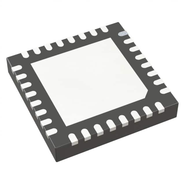
- Part No.:
- ADV7281WBCPZ-MA
- Manufacturer:
- Analog Devices Inc.
- Category:
- CODECS
- Package:
- 32-WFQFN Exposed Pad, CSP
- Datasheet:
-
 ADV7281WBCPZ-MA.pdf
- Description:
- IC VIDEO DECODER 10BIT 32LFCSP
- Quantity:
- Payment:

- Shipping:

Inventory:2,726
Please send an inquiry. Send us your inquiry, and we will respond immediately.
Product details
Overview
ADV7281WBCPZ-MA from Analog Devices is a 10-bit, 4× oversampled SDTV video decoder IC with differential analog video inputs, supporting up to eight CVBS/Y/C/YPrPb input channels and delivering MIPI CSI-2 8-bit YCrCb 4:2:2 output for automotive infotainment and DVR systems.
For engineers reviewing the ADV7281WBCPZ-MA datasheet, ADV7281WBCPZ-MA pinout, ADV7281WBCPZ-MA application, or ADV7281WBCPZ-MA equivalent, key selection considerations include its 8-channel analog input capability, −40°C to +105°C automotive qualification, MIPI CSI-2 interface compliance, and integrated STB diagnostics on two inputs.
Technical Context
The ADV7281WBCPZ-MA implements a fully differential analog front end with on-chip antialiasing filters per channel and supports NTSC/PAL/SECAM autodetection across all input types. Its digital processing block integrates a 5-line adaptive 2D comb filter, CTI enhancement, and ADLLT-based mini-TBC functionality for stable line-locked timing recovery.
It uses a 28.63636 MHz crystal oscillator input (XTALP/XTALN) to drive an internal PLL, generating precise pixel clocks for MIPI CSI-2 transmission at nominal 216 Mbps in interlaced mode. Power domains are segregated: AVDD/DVDD/PVDD at 1.8 V, DVDDIO at 3.3 V, and MVDD at 1.8 V for the MIPI transmitter.
Key Specifications
| Parameter | Value and Actual Design Meaning |
|---|---|
| ADC Resolution | 10-bit with 4× oversampling per channel - enables high-fidelity digitization of composite, S-video, and component analog video signals. |
| Input Channels | 8 fully configurable analog inputs (AIN1–AIN8) - supports multi-camera automotive rearview or surround-view systems without external multiplexing. |
| Output Interface | MIPI CSI-2 compliant serial output - reduces PCB routing complexity versus parallel BT.656, enabling direct connection to mobile/application processors. |
| Video Standards | NTSC/PAL/SECAM autodetection - eliminates manual format configuration and ensures robust operation across global broadcast and legacy video sources. |
| Operating Temperature | −40°C to +105°C - qualified for under-hood or dashboard-mounted automotive applications per AEC-Q100 requirements. |
| Power Supply | DVDDIO = 2.97–3.63 V; AVDD/DVDD/PVDD/MVDD = 1.71–1.89 V - supports low-noise, tightly regulated 1.8 V and 3.3 V rail architectures common in automotive ECUs. |
| Package | 32-lead, 5 mm × 5 mm LFCSP - RoHS-compliant surface-mount package with exposed thermal pad for enhanced heat dissipation in compact modules. |
Pinout & Package
Package: 32-lead, 5 mm × 5 mm, RoHS-compliant LFCSP with exposed thermal pad connected to DGND.
| Pin/Terminal | Circuit Role | Design Meaning |
|---|---|---|
| AIN1–AIN8 | Analog Video Input | Differential/pseudo-differential/single-ended CVBS/Y/C/YPrPb inputs - eight independent channels enable simultaneous multi-source decoding without external switching. |
| XTALP / XTALN | Clock Input | 28.63636 MHz crystal oscillator interface - provides precise reference for internal PLL and pixel clock generation required for MIPI CSI-2 timing compliance. |
| D0P / D0N / CLKP / CLKN | MIPI CSI-2 Output | Differential data and clock lanes - deliver 8-bit YCrCb 4:2:2 video stream at up to 216 Mbps with HS/LP mode transitions per MIPI specification. |
| GPO0–GPO2 | General-Purpose Output | Configurable digital outputs - support system-level control signaling such as camera select, sync pulse generation, or status indication. |
| SCLK / SDATA | I²C Interface | 2-wire serial programming port (400 kHz max) - enables register configuration, format detection status reads, and interrupt handling during runtime. |
| PWRDWN | Power Control | Active-low hardware power-down - reduces total supply current to ≤4.5 μA (MVDD) and ≤73 μA (DVDDIO), critical for low-quiescent automotive subsystems. |
Key Features
| Feature | Design Value |
|---|---|
| 8-channel analog input architecture | Eliminates need for external analog switches in multi-camera systems, reducing BOM count and signal path degradation. |
| Integrated short-to-battery (STB) diagnostics | Enables real-time fault detection on two video inputs - critical for ASIL-B–compliant automotive vision systems requiring functional safety monitoring. |
| Adaptive Digital Line Length Tracking (ADLLT) | Provides mini-time base correction (TBC) without external memory, stabilizing output timing against horizontal jitter in unstable analog sources. |
| 5-line adaptive 2D comb filter | Delivers superior luma/chroma separation in composite video, achieving <0.9° differential phase and <0.5% differential gain distortion. |
| Rovi (Macrovision) copy protection detection | Allows conditional video path management in DRM-aware consumer and commercial media players handling protected content. |
Applications
| Automotive Rearview Camera System | Multi-Channel DVR for Fleet Security |
|---|---|
Use Scenario: Simultaneous decoding of four rear/side-view analog cameras feeding a central display or ADAS ECU. IC Role / Device Role / Timing Role: Primary SDTV video decoder providing synchronized MIPI CSI-2 streams to SoC image signal processor. Use Value: Eight-input capability allows daisy-chained or parallel camera integration; −40°C to +105°C rating ensures reliability in vehicle cabin environments. | Use Scenario: Recording analog video feeds from up to eight surveillance cameras in commercial fleet vehicles. IC Role / Device Role / Timing Role: High-fidelity analog-to-digital conversion with embedded TBC and VBI data slicing for metadata embedding. Use Value: Integrated 2D comb filter and ACE enhance recorded image clarity; MIPI output simplifies interface to ARM-based recording SoCs. |
| Automotive Head-Unit Infotainment | Legacy Video Source Adapter Module |
Use Scenario: Integration of analog backup camera, DVD player, and AV input into a single head-unit display. IC Role / Device Role / Timing Role: Format-agnostic decoder with automatic NTSC/PAL/SECAM detection and seamless input switching. Use Value: Fast switch speed (<100 ms) and autodetection eliminate user format selection; GPO pins enable camera-triggered display overlays. | Use Scenario: Converting legacy composite/S-video outputs from industrial equipment to modern MIPI-based vision processors. IC Role / Device Role / Timing Role: Bridge device translating analog baseband video into standardized mobile interface protocol. Use Value: Eliminates need for custom FPGA-based video interface logic; RoHS LFCSP package supports compact, thermally constrained adapter PCBs. |
Equivalent & Alternatives
The following parts are listed as comparable options for similar SDTV video decoder applications.
| Alternative Part | Technical Difference | Application Difference | Selection Advice |
|---|---|---|---|
| ADV7282-M | Same 8-input architecture and MIPI CSI-2 output, but adds embedded VBI data slicer with closed captioning support and enhanced Rovi detection. | Better suited for broadcast-content-aware systems requiring CC/EIA-608 parsing and advanced copy protection handling. | Select ADV7282-M when VBI metadata extraction or extended Macrovision version compatibility is required. |
| MAX9526 | 10-bit SD decoder with 4-channel input and BT.656 parallel output; no MIPI interface, no STB diagnostics, lower temperature grade (−40°C to +85°C). | Targeted at cost-sensitive consumer media players where parallel interface and non-automotive thermal range are acceptable. | Choose MAX9526 only for non-automotive, non-MIPI designs where BOM cost outweighs interface flexibility and functional safety features. |
Compared with ADV7281WBCPZ-MA, ADV7282-M extends VBI and copy protection capabilities while maintaining pin and software compatibility, whereas MAX9526 offers lower integration and thermal performance-making it unsuitable for automotive deployment despite similar decoding function.
Availability
ADV7281WBCPZ-MA is available at Aetrix Electronics and suitable for automotive infotainment, DVR video security, and smartphone/multimedia handset applications requiring stable component supply, long-term lifecycle support, and AEC-Q100–qualified parts.
Supply support for ADV7281WBCPZ-MA includes scheduled delivery planning, volume procurement assistance, BOM continuity management, traceable sourcing, and lifecycle availability coordination for OEM customers, industrial embedded developers, connected-device designers, and electronics production programs.
Manufacturer
Analog Devices is a global leader in high-performance analog, mixed-signal, and digital signal processing semiconductors, serving industrial, automotive, communications, and consumer markets with precision technology solutions.
The ADV7281WBCPZ-MA belongs to Analog Devices' automotive-qualified video decoder product line, engineered specifically for robust, low-latency SD analog video capture in safety-critical vehicle systems including surround-view and driver assistance platforms.
FAQ
What video standards does the ADV7281WBCPZ-MA support?
The ADV7281WBCPZ-MA supports worldwide NTSC, PAL, and SECAM analog video standards across composite (CVBS), S-video (Y/C), and component (YPrPb) formats. It performs automatic format detection without external configuration, and its 10-bit ADC with 4× oversampling ensures accurate digitization regardless of standard. The ADV7281WBCPZ-MA maintains specified differential phase (<0.9°) and gain (<0.5%) accuracy for all supported standards.
Does the ADV7281WBCPZ-MA support differential video inputs?
Yes, the ADV7281WBCPZ-MA supports fully differential, pseudo-differential, and single-ended analog video inputs on all eight AIN channels. Its analog front end includes on-chip antialiasing filters and delivers excellent common-mode noise rejection (>73 dB CMRR with matched external resistors). This makes the ADV7281WBCPZ-MA ideal for noisy automotive environments where differential signaling improves immunity to EMI.
What is the purpose of the GPO0–GPO2 pins on the ADV7281WBCPZ-MA?
The GPO0, GPO1, and GPO2 pins on the ADV7281WBCPZ-MA are general-purpose outputs configurable via I²C registers to drive external logic, LEDs, or enable signals. They support system-level functions such as camera selection synchronization, interrupt acknowledgment, or status indication in multi-camera automotive systems. Unlike the ADV7281 and ADV7281-M variants, only the ADV7281WBCPZ-MA provides three GPOs-enhancing its flexibility in complex vision subsystems.
How does the ADV7281WBCPZ-MA handle power-down mode?
The ADV7281WBCPZ-MA enters hardware power-down mode when the PWRDWN pin is driven low, reducing total supply current to ≤73 μA on DVDDIO and ≤4.5 μA on MVDD. All internal circuitry-including MIPI transmitter, ADC, and PLL-is disabled while retaining register state if DVDD remains active. This ultra-low quiescent mode meets stringent automotive subsystem sleep-current requirements, and the ADV7281WBCPZ-MA resumes full operation within microseconds upon PWRDWN deassertion.
Is the ADV7281WBCPZ-MA pin-compatible with other members of the ADV7281 family?
No, the ADV7281WBCPZ-MA is not pin-compatible with the ADV7281 or ADV7281-M. While all share the same 32-lead LFCSP package footprint, the ADV7281WBCPZ-MA replaces DIAG1/DIAG2 pins with AIN7/AIN8 and adds GPO0–GPO2, resulting in different pin assignments. Its pinout is identical only to the ADV7281-MA variant. Therefore, board layout must be designed specifically for ADV7281WBCPZ-MA or ADV7281-MA, and the ADV7281WBCPZ-MA cannot serve as a drop-in replacement for earlier family members.
ADV7281WBCPZ-MA Specifications
- Product attributes
- Attribute value
- Manufacturer:
- Analog Devices Inc.
- Series:
- -
- Package/Case:
- 32-WFQFN Exposed Pad, CSP
- Packaging:
- Tray
- Product Status:
- Active
- Type:
- Video
- Data Interface:
- I2C, Serial
- Resolution (Bits):
- 10 b
- Number of ADCs / DACs:
- 1 / 0
- Sigma Delta:
- No
- S/N Ratio, ADCs / DACs (db) Typ:
- -
- Dynamic Range, ADCs / DACs (db) Typ:
- -
- Voltage - Supply, Analog:
- 1.71V ~ 1.89V
- Voltage - Supply, Digital:
- 1.71V ~ 1.89V
- Operating Temperature:
- -40°C ~ 105°C
- Grade:
- Automotive
- Qualification:
- -
- Mounting Type:
- Surface Mount
- Supplier Device Package:
- 32-LFCSP (5x5)
ADV7281WBCPZ-MA FAQ
1.How can I place an order for ADV7281WBCPZ-MA through Aetrix?
Please submit a Request for Quotation (RFQ) for ADV7281WBCPZ-MA on Aetrix. Our sales agent will provide a competitive quotation and guide you through the order confirmation once you accept the terms.
2.Are the price and stock information for ADV7281WBCPZ-MA reliable?
The price and inventory of ADV7281WBCPZ-MA are updated periodically and may fluctuate due to market conditions. Stock and pricing data are typically refreshed every 24 hours. Quotation validity for ADV7281WBCPZ-MA is usually 5 days.
3.What payment methods are accepted for ADV7281WBCPZ-MA?
We accept Wire Transfer, PayPal, Credit Card, Western Union, MoneyGram, and Escrow for ADV7281WBCPZ-MA transactions.
Note: Certain payment methods may incur a processing fee.
4.How is shipping managed for ADV7281WBCPZ-MA?
ADV7281WBCPZ-MA orders can be shipped via leading logistics carriers, including DHL, UPS, FedEx, TNT, or Registered Mail.
Once your ADV7281WBCPZ-MA order is processed, you will receive an email with the shipment details and tracking number.
Note: Tracking information may take up to 24 hours to appear. Express delivery typically takes 3–5 business days.
5.How can I obtain technical support or documentation for ADV7281WBCPZ-MA?
For technical support, including ADV7281WBCPZ-MA datasheets, pinout diagrams, or application guidance, please contact our engineering support team. They can provide detailed documentation and assistance for your ADV7281WBCPZ-MA requirements.
6.How does Aetrix verify that ADV7281WBCPZ-MA is sourced from the original manufacturer or authorized distributors?
All ADV7281WBCPZ-MA products on Aetrix are procured from qualified distributors and authorized channels. Our dedicated quality assurance team conducts strict verification, including traceability checks and, if necessary, third-party testing. This ensures that ADV7281WBCPZ-MA meets industry standards.
7.What is the process for return or replacement of ADV7281WBCPZ-MA?
All ADV7281WBCPZ-MA units undergo pre-shipment inspection (PSI). If there is an issue with ADV7281WBCPZ-MA, returns or replacements are accepted under the following conditions:
1.Quantity discrepancies, incorrect items, or visible external defects (such as breakage or corrosion), acknowledged by Aetrix.
2.The issue is reported within 90 days of delivery.
3.The ADV7281WBCPZ-MA part is unused and in its original packaging.
Return procedure for ADV7281WBCPZ-MA:
1.Submit a request within 90 days.
2.Obtain a Return Material Authorization (RMA) from Aetrix.
ADV7281WBCPZ-MA Tags
-
NAU88C22YG
Nuvoton Technology Corporation

-
TLV320AIC3100IRHBR
Texas Instruments
-
DA7212-01UM2
Renesas
-
NAU8810YG
Nuvoton Technology Corporation
-
DA7218-00U32
Renesas
-
CMX655DQ6-TR1K
CML Micro
-
SGTL5000XNLA3
NXP Semiconductors
-
TLV320AIC3104IRHBR
Texas Instruments
-
MAX9867EWV+T
Analog Devices Inc./Maxim Integrated

-
MAX9860ETG+T
Analog Devices Inc./Maxim Integrated

-
TLV320AIC3106IRGZR
Texas Instruments
-
SGTL5000XNLA3R2
NXP Semiconductors
Tech Hub

A practical engineering guide to 3.3V and 5V logic compatibility, input thresholds, resistor dividers, translator ICs, MOSFET level shifting, I2C pull-ups, timing limits and power-sequencing risks.

The 74HC595 uses push-pull logic outputs, while the TPIC6B595 uses 50 V open-drain DMOS sinks for higher-power loads. This guide compares timing, current limits, 3.3 V interfacing, load wiring, thermal…

The 74HC595 converts serial data into eight stable parallel outputs. This guide covers pin functions, shift and storage timing, OE and MR behavior, drive-current limits, cascading, voltage compatibilit…

A technical comparison of level-sensitive latches and edge-triggered flip-flops, covering timing windows, setup and hold limits, master–slave operation, time borrowing, race-through, HDL inference and…

A D latch stores one bit while Enable controls when data can pass. This reference covers gate-level operation, truth tables, transparency, setup and hold timing, LE versus OE, common ICs and practical …

An SR latch stores one bit through cross-coupled feedback. This engineering reference covers NOR and NAND implementations, truth tables, forbidden-state recovery, gated operation, switch debouncing, fa…

Latch circuits retain one bit through feedback. This technical reference covers SR and D latches, truth tables, transparency, timing limits, latch-versus-flip-flop behavior, applications and common log…

An engineering guide to LED driver operation, constant-current and constant-voltage outputs, linear and switching topologies, dimming, IC selection, calculations, replacement compatibility, and fault c…

Operational amplifier guide covering op amp basics, feedback, ideal vs real op amps, common configurations, buffer circuits, offset, bias current, gain-bandwidth, slew rate, rail-to-rail limits and sel…

Jumper cables guide covering safe connection order, red and black clamp placement, final ground connection, cable gauge, length, clamp quality, copper vs CCA cables, jump starter comparison and battery…


