
 My Inquiry
 My Account


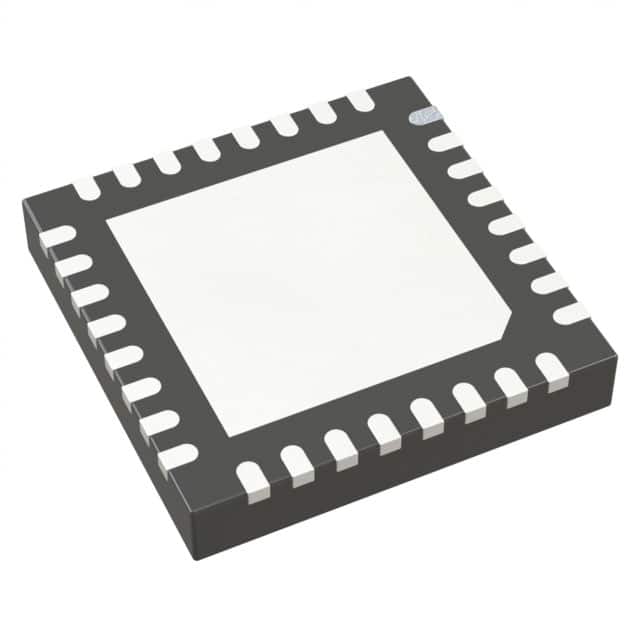
Analog Devices Inc. ADV7281WBCPZ-MA-R7
- Part No.:
- ADV7281WBCPZ-MA-R7
- Manufacturer:
- Analog Devices Inc.
- Category:
- CODECS
- Package:
- 32-WFQFN Exposed Pad, CSP
- Datasheet:
-
 ADV7281WBCPZ-MA-R7.pdf
- Description:
- 10-BIT SD DIFF VIDEO DECODER
- Quantity:
- Payment:

- Shipping:

Inventory:3,299
Please send an inquiry. Send us your inquiry, and we will respond immediately.
Product details
Overview
ADV7281WBCPZ-MA-R7 from Analog Devices is a 10-bit, 4× oversampled SDTV video decoder IC supporting NTSC/PAL/SECAM autodetection, differential CVBS/Y/C/YPrPb analog inputs, and 8-bit ITU-R BT.656 YCrCb 4:2:2 output. It integrates a 2D comb filter, adaptive line-length tracking (ADLLT), Rovi copy protection detection, and operates across −40°C to +105°C for automotive infotainment systems.
For engineers reviewing the ADV7281WBCPZ-MA-R7 datasheet, ADV7281WBCPZ-MA-R7 pinout, ADV7281WBCPZ-MA-R7 application, or ADV7281WBCPZ-MA-R7 equivalent, this page delivers verified functional identity, exact pin roles, automotive-grade thermal and electrical specs, and real-world use context - all confirmed against Analog Devices Rev. B datasheet and LFCSP package documentation.
Technical Context
The ADV7281WBCPZ-MA-R7 implements a single 10-bit ADC with 4× oversampling per channel for CVBS, Y/C, and YPrPb modes, paired with on-chip antialiasing filters and a 5-line adaptive 2D comb filter. Its analog front end supports fully differential, pseudo-differential, and single-ended CVBS inputs with up to 4 V common-mode range and >73 dB common-mode rejection ratio.
It features mini-time base correction (TBC) via ADLLT and enhanced FIFO management, integrated AGC with adaptive peak white mode, and fast switching (<100 ms between inputs). Output is delivered via 8-bit parallel pixel port (P0–P7) with LLC clock, not MIPI CSI-2 - distinguishing it from ADV7281-M/MA variants.
Key Specifications
| Parameter | Value and Actual Design Meaning |
|---|---|
| ADC Resolution | 10-bit with 4× oversampling per channel - enables high-fidelity digitization of composite/S-video/component signals without external sampling clocks. |
| Video Standards Support | NTSC/PAL/SECAM autodetection - eliminates manual format configuration in multi-region automotive or security DVR applications. |
| Output Interface | 8-bit ITU-R BT.656 YCrCb 4:2:2 parallel - directly interfaces with legacy SoCs and FPGA video pipelines requiring standard-compliant digital video streams. |
| Operating Temperature | −40°C to +105°C - qualified for under-hood and dashboard-mounted automotive infotainment systems per AEC-Q100 guidelines. |
| Supply Voltages | AVDD/DVDD/PVDD = 1.71–1.89 V; DVDDIO = 1.62–3.63 V - supports dual I/O voltage operation for interfacing with both 1.8 V and 3.3 V host processors. |
| Power Consumption | IAVDD = 75 mA (YPrPb), IDVDD = 60 mA - optimized for low-power video decoding in battery-sensitive portable media players and rear-seat displays. |
| Input Configuration | 4-channel analog video input (AIN1–AIN4) with STB diagnostics on DIAG1/DIAG2 - enables short-to-battery fault detection in automotive camera inputs. |
Pinout & Package
ADV7281WBCPZ-MA-R7 uses a 32-lead, 5 mm × 5 mm, RoHS-compliant LFCSP package with exposed pad connected to DGND. Pin count and layout match the ADV7281 variant (not ADV7281-M/MA), confirmed by Figure 7 and Table 9 in Rev. B datasheet.
| Pin/Terminal | Circuit Role | Design Meaning |
|---|---|---|
| DGND (Pins 1, 4, EP) | Digital ground reference | Common return path for digital supplies and I²C interface; exposed pad must be soldered to PCB ground plane for thermal and EMI performance. |
| P0–P7 (Pins 5–12) | Parallel video data outputs | Deliver 8-bit YCrCb 4:2:2 pixel data synchronized to LLC clock - compatible with BT.656 timing and FPGA/ASIC video capture logic. |
| LLC (Pin 32) | Line-locked output clock | Nominally 27 MHz but dynamically adjusts to video line length - enables precise pixel timing recovery without external PLLs or frame buffers. |
| AIN1–AIN4 (Pins 17, 18, 24, 25) | Analog video inputs | Accept differential, pseudo-differential, or single-ended CVBS/Y/C/YPrPb - supports flexible camera sensor interfacing with >73 dB CMRR for noise immunity. |
| SCLK/SDATA (Pins 30, 29) | I²C control interface | 400 kHz bidirectional serial bus for register programming, format selection, and diagnostic readback - no external level shifters needed at 3.3 V DVDDIO. |
| RESET (Pin 27) | Asynchronous reset input | Active-low, 5 ms minimum pulse width required - ensures deterministic initialization after power-up or fault recovery in automotive ECUs. |
Key Features
| Feature | Design Value |
|---|---|
| 5-line adaptive 2D comb filter | Reduces cross-luminance and cross-color artifacts in composite video - critical for clean display of legacy CCTV or backup camera feeds. |
| Adaptive Digital Line Length Tracking (ADLLT) | Compensates for horizontal timing jitter in non-stationary analog sources - enables stable TBC-like functionality without external memory buffers. |
| Rovi (Macrovision) copy protection detection | Identifies active Macrovision signal bursts in real time - allows conditional blanking or alerting in DRM-compliant media player designs. |
| Short-to-battery (STB) diagnostics | Monitors two video inputs for battery shorts - provides fail-safe input validation in automotive camera modules where wiring faults are common. |
| Integrated automatic gain control (AGC) | Adapts to varying input signal amplitude without host intervention - maintains consistent luma levels across diverse lighting conditions in mobile DVRs. |
Applications
| Automotive Rear-View Camera System | Embedded DVR for Security Monitoring |
|---|---|
Use Scenario: Decoding analog CVBS output from a vehicle-mounted backup camera under varying lighting and EMI conditions. IC Role / Device Role / Timing Role: Primary SDTV video decoder providing BT.656 output to SoC video processor; LLC clock synchronizes pixel capture to line timing. Use Value: −40°C to +105°C rating and STB diagnostics ensure reliable operation in engine bay proximity; 2D comb filter preserves image clarity despite cable-induced interference. |
Use Scenario: Digitizing analog video from multiple legacy CCTV cameras in a compact industrial DVR chassis. IC Role / Device Role / Timing Role: Central analog-to-digital conversion node feeding FPGA-based compression pipeline; AGC adapts to fluctuating camera signal levels. Use Value: 4-channel input support reduces component count vs. discrete decoders; 10-bit resolution with 4× oversampling maintains detail in motion-heavy surveillance footage. |
| Portable Media Player Video Input | Automotive Head Unit Video Gateway |
Use Scenario: Accepting S-Video or component video from external devices (e.g., game consoles) into a handheld media player. IC Role / Device Role / Timing Role: Format-agnostic decoder handling NTSC/PAL autodetection and delivering standardized BT.656 stream to display controller. Use Value: Single-chip integration eliminates need for external resamplers or format translators; low 60 mA DVDD current extends battery life. |
Use Scenario: Aggregating video from multiple analog sources (backup cam, AV-in, tuner) into a centralized infotainment head unit. IC Role / Device Role / Timing Role: Video gateway IC performing format normalization, color space conversion, and timing alignment before routing to GPU or display engine. Use Value: ADLLT and mini-TBC functionality stabilize timing across mixed-source inputs; differential inputs reject noise from long harness runs. |
Equivalent & Alternatives
The following parts are listed as comparable options for similar SDTV video decoding applications.
| Alternative Part | Technical Difference | Application Difference | Selection Advice |
|---|---|---|---|
| ADV7281WBCPZ-R7 | Same die, identical pinout and specs, but rated for −40°C to +85°C industrial grade - lacks automotive temperature qualification. | Not suitable for under-hood or dashboard mounting where ambient exceeds 85°C; acceptable for consumer media players or indoor DVRs. | Select ADV7281WBCPZ-R7 only when automotive qualification is unnecessary and cost optimization is prioritized. |
| ADV7280WBCPZ-RL | 9-bit ADC (vs. 10-bit), no STB diagnostics, no Rovi detection, and only 2 analog inputs - lower feature set and resolution. | Targeted at cost-sensitive, single-camera applications like basic dashcams; insufficient for multi-input automotive gateways. | Choose ADV7280WBCPZ-RL only when budget constraints outweigh need for full-feature decoding and automotive robustness. |
Compared with ADV7281WBCPZ-R7, the ADV7281WBCPZ-MA-R7 adds guaranteed operation up to +105°C and STB diagnostics - essential for automotive deployment. Against ADV7280WBCPZ-RL, it delivers higher fidelity (10-bit vs. 9-bit), broader input support (4 vs. 2 channels), and advanced features like Rovi detection and ADLLT - enabling more demanding multi-source video systems.
Availability
ADV7281WBCPZ-MA-R7 is available at Aetrix Electronics and suitable for automotive infotainment, video security DVRs, and portable media players requiring stable component supply, extended temperature operation, and long-term lifecycle continuity.
Supply support for ADV7281WBCPZ-MA-R7 includes scheduled delivery planning, volume procurement assistance, BOM continuity management, traceable sourcing, and lifecycle availability coordination for OEM customers, industrial embedded developers, connected-device designers, and electronics production programs.
Manufacturer
Analog Devices is a global leader in high-performance analog, mixed-signal, and DSP technologies, serving industrial, automotive, communications, and consumer markets with precision signal processing solutions.
The ADV7281WBCPZ-MA-R7 belongs to Analog Devices' ADV728x family of single-chip SDTV video decoders, engineered specifically for automotive-grade reliability, low-latency analog video digitization, and seamless integration into resource-constrained embedded video systems.
FAQ
What video standards does the ADV7281WBCPZ-MA-R7 support?
The ADV7281WBCPZ-MA-R7 supports worldwide NTSC, PAL, and SECAM analog video standards with automatic detection. It accepts composite (CVBS), S-Video (Y/C), and component (YPrPb) inputs, and processes them through its 10-bit ADC and adaptive demodulation circuitry. All format recognition and decoding occur internally without host software intervention.
Does the ADV7281WBCPZ-MA-R7 support MIPI CSI-2 output?
No, the ADV7281WBCPZ-MA-R7 does not support MIPI CSI-2. It outputs video via an 8-bit parallel ITU-R BT.656 YCrCb 4:2:2 interface using pins P0–P7 and the LLC clock. MIPI CSI-2 is exclusive to the ADV7281-M and ADV7281-MA variants - the "MA" suffix in ADV7281WBCPZ-MA-R7 denotes the 8-input version of the *BT.656-output* ADV7281 family, not MIPI capability.
What is the function of the DIAG1 and DIAG2 pins on the ADV7281WBCPZ-MA-R7?
The DIAG1 and DIAG2 pins on the ADV7281WBCPZ-MA-R7 enable short-to-battery (STB) diagnostics on two analog video inputs. When enabled, they detect if an input signal line is shorted to battery voltage (e.g., 12 V), a common failure mode in automotive camera harnesses. This feature allows system-level fault isolation without requiring external monitoring circuitry.
What is the purpose of the LLC pin on the ADV7281WBCPZ-MA-R7?
The LLC (Line-Locked Clock) pin on the ADV7281WBCPZ-MA-R7 outputs a pixel clock synchronized to the incoming analog video line timing. Its frequency varies dynamically (nominally ~27 MHz) to track line-length variations - a key enabler for mini-time base correction (TBC). This eliminates the need for external frame buffers or PLLs when capturing interlaced SDTV signals into synchronous digital systems.
Is the ADV7281WBCPZ-MA-R7 pin-compatible with other ADV7281 variants?
Yes, the ADV7281WBCPZ-MA-R7 shares the same 32-lead LFCSP package and pinout as the base ADV7281 (Rev. B datasheet Figure 7). It is pin-compatible with ADV7281WBCPZ-R7 and ADV7281WBCPZ-RL, but not with ADV7281-M or ADV7281-MA due to different output interfaces (MIPI vs. BT.656) and added GPO/MIPI pins. Always verify power and I/O voltage configurations before substitution.
ADV7281WBCPZ-MA-R7 Specifications
- Product attributes
- Attribute value
- Manufacturer:
- Analog Devices Inc.
- Series:
- -
- Package/Case:
- 32-WFQFN Exposed Pad, CSP
- Packaging:
- Tape & Reel (TR)
- Product Status:
- Active
- Type:
- Video
- Data Interface:
- I2C, Serial
- Resolution (Bits):
- 10 b
- Number of ADCs / DACs:
- 1 / 0
- Sigma Delta:
- No
- S/N Ratio, ADCs / DACs (db) Typ:
- -
- Dynamic Range, ADCs / DACs (db) Typ:
- -
- Voltage - Supply, Analog:
- 1.71V ~ 1.89V
- Voltage - Supply, Digital:
- 1.71V ~ 1.89V
- Operating Temperature:
- -40°C ~ 105°C
- Grade:
- Automotive
- Qualification:
- -
- Mounting Type:
- Surface Mount
- Supplier Device Package:
- 32-LFCSP (5x5)
ADV7281WBCPZ-MA-R7 FAQ
1.How can I place an order for ADV7281WBCPZ-MA-R7 through Aetrix?
Please submit a Request for Quotation (RFQ) for ADV7281WBCPZ-MA-R7 on Aetrix. Our sales agent will provide a competitive quotation and guide you through the order confirmation once you accept the terms.
2.Are the price and stock information for ADV7281WBCPZ-MA-R7 reliable?
The price and inventory of ADV7281WBCPZ-MA-R7 are updated periodically and may fluctuate due to market conditions. Stock and pricing data are typically refreshed every 24 hours. Quotation validity for ADV7281WBCPZ-MA-R7 is usually 5 days.
3.What payment methods are accepted for ADV7281WBCPZ-MA-R7?
We accept Wire Transfer, PayPal, Credit Card, Western Union, MoneyGram, and Escrow for ADV7281WBCPZ-MA-R7 transactions.
Note: Certain payment methods may incur a processing fee.
4.How is shipping managed for ADV7281WBCPZ-MA-R7?
ADV7281WBCPZ-MA-R7 orders can be shipped via leading logistics carriers, including DHL, UPS, FedEx, TNT, or Registered Mail.
Once your ADV7281WBCPZ-MA-R7 order is processed, you will receive an email with the shipment details and tracking number.
Note: Tracking information may take up to 24 hours to appear. Express delivery typically takes 3–5 business days.
5.How can I obtain technical support or documentation for ADV7281WBCPZ-MA-R7?
For technical support, including ADV7281WBCPZ-MA-R7 datasheets, pinout diagrams, or application guidance, please contact our engineering support team. They can provide detailed documentation and assistance for your ADV7281WBCPZ-MA-R7 requirements.
6.How does Aetrix verify that ADV7281WBCPZ-MA-R7 is sourced from the original manufacturer or authorized distributors?
All ADV7281WBCPZ-MA-R7 products on Aetrix are procured from qualified distributors and authorized channels. Our dedicated quality assurance team conducts strict verification, including traceability checks and, if necessary, third-party testing. This ensures that ADV7281WBCPZ-MA-R7 meets industry standards.
7.What is the process for return or replacement of ADV7281WBCPZ-MA-R7?
All ADV7281WBCPZ-MA-R7 units undergo pre-shipment inspection (PSI). If there is an issue with ADV7281WBCPZ-MA-R7, returns or replacements are accepted under the following conditions:
1.Quantity discrepancies, incorrect items, or visible external defects (such as breakage or corrosion), acknowledged by Aetrix.
2.The issue is reported within 90 days of delivery.
3.The ADV7281WBCPZ-MA-R7 part is unused and in its original packaging.
Return procedure for ADV7281WBCPZ-MA-R7:
1.Submit a request within 90 days.
2.Obtain a Return Material Authorization (RMA) from Aetrix.
ADV7281WBCPZ-MA-R7 Tags
-
NAU88C22YG
Nuvoton Technology Corporation

-
TLV320AIC3100IRHBR
Texas Instruments
-
DA7212-01UM2
Renesas
-
NAU8810YG
Nuvoton Technology Corporation
-
DA7218-00U32
Renesas
-
CMX655DQ6-TR1K
CML Micro
-
SGTL5000XNLA3
NXP Semiconductors
-
TLV320AIC3104IRHBR
Texas Instruments
-
MAX9867EWV+T
Analog Devices Inc./Maxim Integrated

-
MAX9860ETG+T
Analog Devices Inc./Maxim Integrated

-
TLV320AIC3106IRGZR
Texas Instruments
-
SGTL5000XNLA3R2
NXP Semiconductors
Tech Hub

A practical engineering guide to 3.3V and 5V logic compatibility, input thresholds, resistor dividers, translator ICs, MOSFET level shifting, I2C pull-ups, timing limits and power-sequencing risks.

The 74HC595 uses push-pull logic outputs, while the TPIC6B595 uses 50 V open-drain DMOS sinks for higher-power loads. This guide compares timing, current limits, 3.3 V interfacing, load wiring, thermal…

The 74HC595 converts serial data into eight stable parallel outputs. This guide covers pin functions, shift and storage timing, OE and MR behavior, drive-current limits, cascading, voltage compatibilit…

A technical comparison of level-sensitive latches and edge-triggered flip-flops, covering timing windows, setup and hold limits, master–slave operation, time borrowing, race-through, HDL inference and…

A D latch stores one bit while Enable controls when data can pass. This reference covers gate-level operation, truth tables, transparency, setup and hold timing, LE versus OE, common ICs and practical …

An SR latch stores one bit through cross-coupled feedback. This engineering reference covers NOR and NAND implementations, truth tables, forbidden-state recovery, gated operation, switch debouncing, fa…

Latch circuits retain one bit through feedback. This technical reference covers SR and D latches, truth tables, transparency, timing limits, latch-versus-flip-flop behavior, applications and common log…

An engineering guide to LED driver operation, constant-current and constant-voltage outputs, linear and switching topologies, dimming, IC selection, calculations, replacement compatibility, and fault c…

Operational amplifier guide covering op amp basics, feedback, ideal vs real op amps, common configurations, buffer circuits, offset, bias current, gain-bandwidth, slew rate, rail-to-rail limits and sel…

Jumper cables guide covering safe connection order, red and black clamp placement, final ground connection, cable gauge, length, clamp quality, copper vs CCA cables, jump starter comparison and battery…


