
 My Inquiry
 My Account


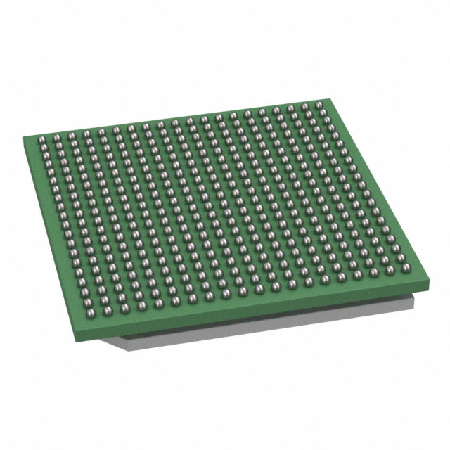
Texas Instruments AFE7444IALK
- Part No.:
- AFE7444IALK
- Manufacturer:
- Texas Instruments
- Category:
- Analog Front End (AFE)
- Package:
- 400-BFBGA, FCBGA
- Datasheet:
-
 AFE7444IALK.pdf
- Description:
- DUAL-CHANNEL RF SAMPLING TRANSC
- Quantity:
- Payment:

- Shipping:

Inventory:3,602
Please send an inquiry. Send us your inquiry, and we will respond immediately.
Product details
Overview
AFE7444IALK from Texas Instruments is a quad-channel, RF-sampling analog front end (AFE) integrating four 14-bit, 9-GSPS DACs and four 14-bit, 3-GSPS ADCs. It supports 10 MHz–6 GHz RF operation with up to 800-MHz signal bandwidth per channel, dual DUC/DDC paths, JESD204B subclass-1 interface (8 TX + 8 RX lanes at 15 Gbps), and on-chip PLL/VCO - enabling direct C-band sampling in wideband communications and test equipment.
For engineers reviewing the AFE7444IALK datasheet, AFE7444IALK pinout, AFE7444IALK application, or AFE7444IALK equivalent, key selection criteria include RF frequency range (10 MHz–6 GHz), DAC/ADC sampling rates (9 GSPS / 3 GSPS), JESD204B lane count and subclass compliance, power detector integration, and FCBGA-400 package thermal and layout constraints.
Technical Context
The AFE7444IALK implements two independent digital upconverters (DUC) per DAC channel with 32-bit NCOs, interpolation ratios from 8× to 36×, Sin(x)/x correction, and configurable delay - supporting wideband waveform synthesis with coherent multi-channel phase alignment. Each DAC path includes one digital step attenuator (DSA) for output power tuning.
Each ADC channel integrates dual digital downconverters (DDC) with 3-phase coherent 32-bit NCOs, decimation from 3× to 32×, two DSAs, and integrated RF/digital power detectors. The JESD204B interface provides 8 transceiver lanes (TX+RX) with subclass-1 multichip synchronization for deterministic latency and sample alignment across channels.
Key Specifications
| Parameter | Value and Actual Design Meaning |
|---|---|
| DAC resolution & rate | 14-bit, 9 GSPS - enables high-fidelity wideband signal generation up to 800-MHz instantaneous bandwidth per channel |
| ADC resolution & rate | 14-bit, 3 GSPS - supports high-dynamic-range digitization of RF signals up to 6 GHz with –151 dBFS/Hz NSD |
| RF frequency range | 10 MHz to 6 GHz - allows direct sampling in L-, S-, and C-bands without analog up/down-conversion stages |
| JESD204B interface | 8 TX + 8 RX lanes, up to 15 Gbps, subclass-1 - ensures deterministic latency and synchronized multi-device timing |
| Digital signal processing | Dual DUC per DAC (8×–36× interp); dual DDC per ADC (3×–32× decim); 32-bit NCOs - enables flexible spectral placement and channelization |
| Power dissipation | 1.7 W/ch (DAC @ 9 GSPS), 1.8 W/ch (ADC @ 3 GSPS) - defines thermal management requirements for high-density RF systems |
| Package | FCBGA-400, 17 mm × 17 mm, 0.8-mm pitch - requires controlled-depth solder paste, exposed thermal pad, and strict reflow profile adherence |
Pinout & Package
AFE7444IALK uses a 400-ball flip-chip ball grid array (FCBGA) package with 17 mm × 17 mm body size, 0.8-mm ball pitch, and maximum height of 2.65 mm. The package features an exposed thermal pad on the bottom side and Pb-free die bump with SnPb solder balls (per ALK0400A mechanical drawing).
| Pin/Terminal | Circuit Role | Design Meaning |
|---|---|---|
| CLKP / CLKM | Differential reference clock input | Accepts LVDS/LVPECL-compatible clock; feeds internal PLL for system timing generation |
| SYSREFP / SYSREFM | Differential JESD204B subclass-1 synchronization input | Aligns sample clocks and frame boundaries across multiple AFE7444IALK devices |
| SRX1P–SRX8M | ADC serial receiver (JESD204B RX) lanes | 8-lane JESD204B RX interface receiving digitized data from external FPGA/processor |
| STX1P–STX8M | DAC serial transmitter (JESD204B TX) lanes | 8-lane JESD204B TX interface delivering waveform data to DACs with deterministic latency |
| RXA/RXCDSA1P–RXB/RXDDSA2M | Dual DSA control inputs per ADC channel | Configures attenuation steps for RF and digital power detection paths independently |
| TXAP/TXCP–TXBM/TXDM | DAC analog differential outputs | Four fully differential RF outputs (2 per DAC pair), DC-coupled, ±1.8-V swing capability |
| SPI / JTAG / GPIO | Configuration and debug interface | 4-wire SPI configures registers; JTAG enables boundary scan; GPIO supports sync/trigger functions |
Key Features
| Feature | Design Value |
|---|---|
| Dual DUC per DAC with Sin(x)/x correction | Compensates DAC image response in wideband transmit paths, preserving signal fidelity up to Nyquist |
| Dual DDC per ADC with 3-phase coherent NCOs | Enables simultaneous frequency translation of multiple bands with phase coherence across all four channels |
| Integrated RF and digital power detectors | Provides real-time monitoring of signal amplitude at RF and baseband levels for closed-loop PA protection and AGC |
| On-chip PLL with bypass option | Reduces external clocking complexity; supports single-ended or differential reference; VCO operates up to 3 GHz |
| Fast frequency hopping & PAP logic | Hops < 1 µs between frequencies; power amplifier protection triggers DAC shutdown within 100 ns upon over-power detection |
Applications
| 5G Massive MIMO Base Stations | Wideband RF Test Equipment |
|---|---|
|
Use Scenario: Transmitting and receiving multiple spatial streams across 3.3–4.2 GHz band with real-time beamforming and calibration. IC Role / Device Role / Timing Role: AFE7444IALK serves as the RF-sampling front end for both uplink and downlink paths, providing synchronized 4T4R operation with deterministic JESD204B latency. Use Value: Eliminates analog up/down-converters and local oscillators, reducing BOM cost and PCB area while enabling full 800-MHz instantaneous bandwidth per channel. |
Use Scenario: Generating and analyzing complex wideband waveforms (e.g., 5G NR FR1, radar chirps) in automated test systems. IC Role / Device Role / Timing Role: AFE7444IALK acts as a high-speed arbitrary waveform generator and digitizer, leveraging dual DUC/DDC and NCOs for precise spectral positioning. Use Value: Achieves >73 dBc SFDR and –151 dBFS/Hz NSD, meeting demanding spectral purity and dynamic range requirements for metrology-grade instruments. |
| Phased Array Radar Systems | Electronic Warfare Signal Generators |
|
Use Scenario: Coherent multi-channel transmission and reception for adaptive beam steering and clutter suppression in X-band radar. IC Role / Device Role / Timing Role: AFE7444IALK provides four synchronized RF channels with sub-nanosecond inter-channel skew via subclass-1 JESD204B and shared SYSREF. Use Value: Enables real-time phase and amplitude calibration across all channels using integrated power detectors and DSA controls. |
Use Scenario: Jamming signal synthesis with rapid frequency agility and low-latency reconfiguration in tactical EW platforms. IC Role / Device Role / Timing Role: AFE7444IALK functions as a wideband agile synthesizer, using fast-hopping DUCs and on-chip PLL to switch frequencies in <1 µs. Use Value: Supports threat library replay with minimal latency overhead and no external LO switching, improving response time against dynamic emitters. |
Equivalent & Alternatives
The following parts are listed as comparable options for similar RF-sampling AFE applications.
| Alternative Part | Technical Difference | Application Difference | Selection Advice |
|---|---|---|---|
| AFE7422IABJ | 2-channel version (2× DAC + 2× ADC), same 14-bit/9-GSPS & 14-bit/3-GSPS specs, identical JESD204B subclass-1 support | Lower channel count reduces PCB area and power; suitable for dual-stream or cost-sensitive 2T2R systems | Select AFE7422IABJ when system requires only two transmit/receive channels and space/power budgets are constrained |
| AFE7769IABJ | Quad-channel with higher DAC rate (10.2 GSPS), wider RF range (up to 10 GHz), added DSA per DAC path, and enhanced clocking flexibility | Supports Ka-band and mmWave extension; requires tighter jitter control and more complex thermal design | Choose AFE7769IABJ for next-generation systems requiring >6 GHz coverage or improved SFDR beyond 91 dBc worst spur |
Compared with AFE7444IALK, AFE7422IABJ offers half the channel density at identical per-channel performance, while AFE7769IABJ extends RF range and sampling rate but increases layout and thermal complexity - making AFE7444IALK optimal for balanced C-band 4T4R systems requiring proven reliability and mature toolchain support.
Availability
AFE7444IALK is available at Aetrix Electronics and suitable for 5G infrastructure, wideband test instrumentation, and phased-array radar systems requiring stable component supply, long-term lifecycle assurance, and traceable sourcing.
Supply support for AFE7444IALK includes scheduled delivery planning, volume procurement assistance, BOM continuity management, traceable sourcing, and lifecycle availability coordination for OEM customers, industrial embedded developers, connected-device designers, and electronics production programs.
Manufacturer
Texas Instruments is a global semiconductor company specializing in analog and embedded processing technologies, with leadership in high-speed data converters, RF solutions, and precision analog ICs.
The AFE7444IALK belongs to TI's high-performance RF-sampling AFE product line, designed specifically for wideband communications, defense radar, and test equipment where direct RF sampling eliminates analog mixing stages and improves system agility.
FAQ
What is the RF frequency range supported by the AFE7444IALK?
The AFE7444IALK supports an RF frequency range from 10 MHz to 6 GHz. This enables direct sampling in L-, S-, and C-bands without requiring external up/down-conversion circuitry. Its architecture is optimized for wideband applications such as 5G base stations and radar, where avoiding analog mixers improves signal integrity and reduces system complexity. The AFE7444IALK maintains specified AC performance - including SNR and SFDR - across this full range under defined operating conditions.
Does the AFE7444IALK include integrated clock generation?
Yes, the AFE7444IALK includes an on-chip PLL with integrated VCO capable of generating clocks up to 3 GHz. It supports both internal clock synthesis and external clock bypass modes, offering flexibility in system clock architecture. The PLL accepts differential reference inputs (CLKP/CLKM) and provides programmable clock dividers for generating multiple internal clock domains. This integrated clocking reduces external component count and simplifies timing design for JESD204B subclass-1 synchronization in the AFE7444IALK.
How many JESD204B lanes does the AFE7444IALK support, and what subclass is implemented?
The AFE7444IALK supports eight JESD204B transmitter lanes and eight receiver lanes, operating at up to 15 Gbps per lane. It implements subclass-1 compliance, ensuring deterministic latency and precise multi-device synchronization via SYSREFP/SYSREFM signals. This capability allows tightly coordinated operation across multiple AFE7444IALK devices in phased-array or MIMO systems. The AFE7444IALK's subclass-1 implementation is validated per JEDEC standard and used in production 5G and radar platforms.
What power supply voltages are required for the AFE7444IALK?
The AFE7444IALK requires five distinct supply rails: 1.8 V (digital I/O), 1.5 V (JESD204B core), 1.15 V (ADC/DAC digital core), 1.0 V (PLL/VCO), and ±1.8 V (analog output drivers). An additional 1.85 V rail powers the GPIO and SPI interface. These voltages must be sequenced during power-up per TI's recommended sequence to prevent latch-up or configuration failure. The AFE7444IALK's power delivery network must meet tight ripple and noise specifications - especially on the 1.15-V and 1.0-V rails - to maintain specified SNR and SFDR performance.
Is the AFE7444IALK pin-compatible with other devices in the AFE74xx family?
No, the AFE7444IALK is not pin-compatible with other AFE74xx variants such as AFE7422IABJ or AFE7444IABJ. While all share the same FCBGA-400 footprint (17 mm × 17 mm), ball assignments differ significantly - particularly for analog I/O, power domains, and JESD204B lane mapping. The AFE7444IALK uses the ALK package variant with SnPb solder balls and distinct thermal pad configuration, whereas ABJ variants use Pb-free balls. Board designs must be validated separately for each part number; the AFE7444IALK requires its own layout and power delivery design.
AFE7444IALK Specifications
- Product attributes
- Attribute value
- Manufacturer:
- Texas Instruments
- package:
- 400-BFBGA, FCBGA
- Series:
- -
- Packaging:
- Tray
- Product Status:
- Active
- Number of Bits:
- 14
- Number of Channels:
- 4
- Power (Watts):
- -
- Voltage - Supply, Analog:
- -
- Voltage - Supply, Digital:
- -
- Mounting Type:
- Surface Mount
- Grade:
- -
- Qualification:
- -
AFE7444IALK FAQ
1.How can I place an order for AFE7444IALK through Aetrix?
Please submit a Request for Quotation (RFQ) for AFE7444IALK on Aetrix. Our sales agent will provide a competitive quotation and guide you through the order confirmation once you accept the terms.
2.Are the price and stock information for AFE7444IALK reliable?
The price and inventory of AFE7444IALK are updated periodically and may fluctuate due to market conditions. Stock and pricing data are typically refreshed every 24 hours. Quotation validity for AFE7444IALK is usually 5 days.
3.What payment methods are accepted for AFE7444IALK?
We accept Wire Transfer, PayPal, Credit Card, Western Union, MoneyGram, and Escrow for AFE7444IALK transactions.
Note: Certain payment methods may incur a processing fee.
4.How is shipping managed for AFE7444IALK?
AFE7444IALK orders can be shipped via leading logistics carriers, including DHL, UPS, FedEx, TNT, or Registered Mail.
Once your AFE7444IALK order is processed, you will receive an email with the shipment details and tracking number.
Note: Tracking information may take up to 24 hours to appear. Express delivery typically takes 3–5 business days.
5.How can I obtain technical support or documentation for AFE7444IALK?
For technical support, including AFE7444IALK datasheets, pinout diagrams, or application guidance, please contact our engineering support team. They can provide detailed documentation and assistance for your AFE7444IALK requirements.
6.How does Aetrix verify that AFE7444IALK is sourced from the original manufacturer or authorized distributors?
All AFE7444IALK products on Aetrix are procured from qualified distributors and authorized channels. Our dedicated quality assurance team conducts strict verification, including traceability checks and, if necessary, third-party testing. This ensures that AFE7444IALK meets industry standards.
7.What is the process for return or replacement of AFE7444IALK?
All AFE7444IALK units undergo pre-shipment inspection (PSI). If there is an issue with AFE7444IALK, returns or replacements are accepted under the following conditions:
1.Quantity discrepancies, incorrect items, or visible external defects (such as breakage or corrosion), acknowledged by Aetrix.
2.The issue is reported within 90 days of delivery.
3.The AFE7444IALK part is unused and in its original packaging.
Return procedure for AFE7444IALK:
1.Submit a request within 90 days.
2.Obtain a Return Material Authorization (RMA) from Aetrix.
AFE7444IALK Tags
-
MCP3911A0-E/SS
Microchip Technology
-
ADS131A04IPBSR
Texas Instruments
-
ADS1292RIPBSR
Texas Instruments
-
ADS1292IRSMT
Texas Instruments

-
LMP90097MHE/NOPB
Texas Instruments
-
AD5940BCBZ-RL
Analog Devices Inc.
-
AD5940BCBZ-RL7
Analog Devices Inc.
-
AD5941BCPZ-RL7
Analog Devices Inc.
-
AD5941BCPZ
Analog Devices Inc.
-
ADS131E08IPAGR
Texas Instruments

-
LMP90100MH/NOPB
Texas Instruments
-
LMP90100MHE/NOPB
Texas Instruments
Tech Hub

A practical engineering guide to 3.3V and 5V logic compatibility, input thresholds, resistor dividers, translator ICs, MOSFET level shifting, I2C pull-ups, timing limits and power-sequencing risks.

The 74HC595 uses push-pull logic outputs, while the TPIC6B595 uses 50 V open-drain DMOS sinks for higher-power loads. This guide compares timing, current limits, 3.3 V interfacing, load wiring, thermal…

The 74HC595 converts serial data into eight stable parallel outputs. This guide covers pin functions, shift and storage timing, OE and MR behavior, drive-current limits, cascading, voltage compatibilit…

A technical comparison of level-sensitive latches and edge-triggered flip-flops, covering timing windows, setup and hold limits, master–slave operation, time borrowing, race-through, HDL inference and…

A D latch stores one bit while Enable controls when data can pass. This reference covers gate-level operation, truth tables, transparency, setup and hold timing, LE versus OE, common ICs and practical …

An SR latch stores one bit through cross-coupled feedback. This engineering reference covers NOR and NAND implementations, truth tables, forbidden-state recovery, gated operation, switch debouncing, fa…

Latch circuits retain one bit through feedback. This technical reference covers SR and D latches, truth tables, transparency, timing limits, latch-versus-flip-flop behavior, applications and common log…

An engineering guide to LED driver operation, constant-current and constant-voltage outputs, linear and switching topologies, dimming, IC selection, calculations, replacement compatibility, and fault c…

Operational amplifier guide covering op amp basics, feedback, ideal vs real op amps, common configurations, buffer circuits, offset, bias current, gain-bandwidth, slew rate, rail-to-rail limits and sel…

Jumper cables guide covering safe connection order, red and black clamp placement, final ground connection, cable gauge, length, clamp quality, copper vs CCA cables, jump starter comparison and battery…


