
 My Inquiry
 My Account


Alpha & Omega Semiconductor Inc. AOZ1336DI
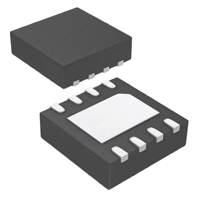
- Part No.:
- AOZ1336DI
- Manufacturer:
- Alpha & Omega Semiconductor Inc.
- Package:
- 8-WFDFN Exposed Pad
- Datasheet:
-
 AOZ1336DI.pdf
- Description:
- IC PWR SWITCH N-CHAN 1:1 8DFN
- Quantity:
- Payment:

- Shipping:

Inventory:3,754
Please send an inquiry. Send us your inquiry, and we will respond immediately.
Product details
Overview
AOZ1336DI from Alpha and Omega Semiconductor is a single-channel smart load switch integrating an n-channel MOSFET with 27 mΩ typical RDS(ON), supporting 4 A continuous current at input voltages from 0.8 V to 5.5 V and bias supply of 2.5 V to 5 V. It features independent ON-pin control, integrated 220 Ω output discharge resistor, thermal shutdown, and adjustable slew rate via external CT capacitor - deployed in portable computing power rail sequencing.
For engineers reviewing the AOZ1336DI datasheet, pinout, applications, or equivalent options, key selection considerations include its DFN-8L thermal pad package, VIN ≤ VBIAS dependency for low RDS(ON), quiescent current of 50 µA, and precise turn-on/off timing control across varying input and bias conditions.
Technical Context
The AOZ1336DI implements a charge-pump–assisted gate driver architecture to maintain low on-resistance across wide VIN (0.8–5.5 V) and VBIAS (2.5–5.5 V) ranges, requiring VIN ≤ VBIAS for optimal 27 mΩ RDS(ON). Its internal logic accepts TTL/CMOS-compatible ON-pin signals (VONH = 1.2 V, VONL = 0.5 V) to enable/disable the main NFET path.
Output slew rate is externally programmable via CT pin capacitance, enabling controlled voltage ramping (e.g., 22 µs rise time at 0.8 V with 220 pF), while integrated 220 Ω pull-down ensures rapid VOUT discharge (<100 µs) when disabled. Thermal shutdown activates at 180°C junction temperature with 130°C hysteresis.
Key Specifications
| Parameter | Value and Actual Design Meaning |
|---|---|
| Input Voltage Range | 0.8 V to 5.5 V - supports ultra-low-voltage rails (e.g., 1.2 V I/O domains) and standard 3.3 V/5 V systems. |
| Continuous Current | 4 A - sustains full-rated load without derating at TA = 85°C with proper PCB thermal design. |
| RDS(ON) | 27 mΩ typ. at VBIAS ≥ VIN - enables <100 mW conduction loss at 2 A, critical for battery-powered efficiency. |
| Quiescent Current | 50 µA - minimizes standby power draw in always-on subsystems like USB-C port controllers. |
| Thermal Shutdown | 180°C activation / 130°C recovery - protects against sustained overload or poor heatsinking in compact enclosures. |
| Package | 2 mm × 2 mm DFN-8L with exposed thermal pad - achieves θJA = 90°C/W and θJC = 12°C/W for high-power density mounting. |
| Output Discharge | Integrated 220 Ω resistor - discharges output to <10% VOUT within 100 µs, preventing floating bus states during hot-swap. |
Pinout & Package
AOZ1336DI uses a thermally enhanced 2 mm × 2 mm DFN-8L package with bottom-exposed pad (EPAD) that must be soldered to GND for thermal and electrical integrity. The package supports reflow assembly per JEDEC J-STD-020 and achieves 12°C/W junction-to-case thermal resistance.
| Pin/Terminal | Circuit Role | Design Meaning |
|---|---|---|
| 1, 2 - IN | Power input node | Bypass with ≥1 µF ceramic capacitor close to pins to suppress inrush-induced voltage droop during turn-on. |
| 3 - ON | Enable control input | TTL/CMOS-compatible logic input; active-high with 1.2 V threshold ensures robust noise immunity in noisy digital environments. |
| 4 - VBIAS | Bias supply input | Must be 2.5–5.5 V and ≥ VIN to achieve specified 27 mΩ RDS(ON); powers internal charge pump and logic. |
| 5 - GND | Ground reference | Common return for IN, OUT, VBIAS, and EPAD; requires low-impedance connection to minimize ground bounce. |
| 6 - CT | Slew rate programming node | Connects external capacitor to GND; sets VOUT rise/fall time (e.g., 220 pF yields ~22 µs at 0.8 V). |
| 7, 8 - OUT | Switched output node | Delivers regulated load current; connects to downstream circuitry and ≥0.1 µF output capacitor for transient stability. |
| EPAD | Thermal & electrical ground | Exposed copper pad under package body; must be fully soldered to large GND plane for thermal dissipation and EMI reduction. |
Key Features
| Feature | Design Value |
|---|---|
| Adjustable output slew rate | External CT capacitor tunes rise/fall times from <10 µs to >16 ms - prevents inrush current spikes and EMI in sensitive analog or RF subsystems. |
| Integrated quick output discharge | 220 Ω internal resistor pulls OUT to GND within 100 µs after disable - eliminates floating outputs during hot-plug or power sequencing. |
| Low quiescent current | 50 µA at VBIAS = 5 V - extends battery life in always-on circuits such as wake-on-LAN or sensor hub supervisors. |
| Thermal shutdown with hysteresis | 180°C trip / 130°C reset - provides self-recovery protection during temporary overloads without requiring system-level intervention. |
| VIN ≤ VBIAS optimized RDS(ON) | 27 mΩ maintained across 0.8–5.5 V VIN when VBIAS ≥ VIN - ensures consistent efficiency regardless of input rail variation. |
Applications
| Portable Computing Power Rail Control | Ultrabook USB-C Port Management |
|---|---|
|
Use Scenario: Sequencing 3.3 V and 5 V rails for CPU I/O, display interface, and peripheral controllers in thin-and-light notebooks. IC Role / Device Role / Timing Role: Smart load switch providing controlled power-up/down with programmable slew rate and fast output discharge. Use Value: Prevents bus contention and inrush-induced brownouts during multi-rail sequencing, improving system boot reliability. |
Use Scenario: Enabling/disabling VBUS and configuration channel (CC) power in USB-C receptacles during plug detection and role negotiation. IC Role / Device Role / Timing Role: Single-channel load switch with ON-pin logic control and thermal protection for hot-swap-safe port power delivery. Use Value: Enables rapid, safe power cycling of USB-C ports without firmware intervention or external discharge circuitry. |
| Tablet PC Display Backlight Supply | SSD Power Domain Isolation |
|
Use Scenario: Switching 5 V backlight LED driver supply in response to display on/off commands in tablet PCs. IC Role / Device Role / Timing Role: Load switch with adjustable rise time to limit inrush into large capacitive backlight loads. Use Value: Eliminates visible flash or flicker during backlight turn-on by controlling dV/dt to match human visual persistence. |
Use Scenario: Isolating 3.3 V VCCQ and 1.2 V VPP power domains in NVMe SSD modules during sleep/wake transitions. IC Role / Device Role / Timing Role: Low-RDS(ON) load switch with fast turn-off and integrated discharge for clean domain power gating. Use Value: Reduces standby leakage by >95% and ensures deterministic power-state transitions without external RC networks. |
Equivalent & Alternatives
The following parts are listed as comparable options for similar smart load switch applications.
| Alternative Part | Technical Difference | Application Difference | Selection Advice |
|---|---|---|---|
| TPS22916BLYFPR | Lower 22 mΩ RDS(ON) but fixed 1.2 V minimum VIN; no CT pin for slew control; 1.5 A max current. | Best suited for low-current, fixed-VIN applications where precise timing control is unnecessary. | Select when prioritizing lowest possible RDS(ON) at 1.2–5.5 V and footprint compatibility matters more than slew adjustability. |
| RT9711CGJ5 | Higher 45 mΩ RDS(ON); no integrated discharge resistor; requires external pull-down for VOUT discharge. | Used in cost-sensitive consumer electronics where thermal performance and board space are secondary to BOM count. | Choose only if board area allows external 220 Ω resistor and system tolerates slower discharge (>1 ms) and higher conduction loss. |
Compared with TPS22916BLYFPR and RT9711CGJ5, the AOZ1336DI uniquely combines 4 A capability, adjustable slew rate, integrated discharge, and operation down to 0.8 V - making it optimal for high-density, multi-rail portable systems requiring precise power sequencing and thermal resilience.
Availability
AOZ1336DI is available at Aetrix Electronics and suitable for portable computing power rail control, ultrabook USB-C port management, tablet PC display backlight supply, SSD power domain isolation, and telecom/datacom board-level power gating requiring stable component supply and long-term lifecycle support.
Supply support for AOZ1336DI includes scheduled delivery planning, volume procurement assistance, BOM continuity management, traceable sourcing, and lifecycle availability coordination for OEM customers, industrial embedded developers, connected-device designers, and electronics production programs.
Manufacturer
Alpha and Omega Semiconductor (AOS) is a fabless power semiconductor company specializing in high-efficiency MOSFETs, load switches, and power ICs for computing, consumer, and industrial markets.
The AOZ1336DI belongs to AOS's smart load switch product line, designed specifically for compact, high-current power rail sequencing in space-constrained portable electronics with stringent thermal and EMI requirements.
FAQ
What is the minimum input voltage supported by the AOZ1336DI?
The AOZ1336DI supports an input voltage range from 0.8 V to 5.5 V. This ultra-low 0.8 V minimum enables direct integration with sub-1 V processor I/O domains and advanced low-power SoC rails, provided VBIAS remains ≥ VIN and within its 2.5–5.5 V operating window. Operation below 0.8 V is not characterized or guaranteed.
How does the CT pin affect AOZ1336DI switching behavior?
The CT pin on the AOZ1336DI sets output slew rate by connecting an external capacitor to GND. Larger CT values increase rise/fall times - e.g., 220 pF yields ~22 µs at 0.8 V, while 1000 pF extends it to ~1.6 ms. This programmability prevents inrush current peaks and EMI during turn-on, directly shaping VOUT transient response per application needs.
Does the AOZ1336DI require an external discharge resistor?
No, the AOZ1336DI integrates a 220 Ω internal pull-down resistor between OUT and GND. When the device is disabled (ON = low), this resistor actively discharges the output node to <10% of VOUT within 100 µs, eliminating the need for external components and ensuring clean, predictable power-down behavior in hot-swap or sequencing applications.
What thermal derating applies to AOZ1336DI at 85°C ambient?
At TA = +85°C, the AOZ1336DI maintains its full 4 A continuous current rating only with adequate PCB thermal design - specifically, a 2-layer board with ≥1 in² copper pour connected to the EPAD and minimal trace resistance. Without thermal enhancement, current must be reduced per the RDS(ON)-vs-TJ curve and θJA = 90°C/W specification to keep TJ ≤ 150°C.
Can AOZ1336DI operate with VIN greater than VBIAS?
Yes, the AOZ1336DI can operate with VIN > VBIAS, but RDS(ON) increases significantly - e.g., rising from 27 mΩ (typ.) to >33 mΩ when VIN exceeds VBIAS. For optimal efficiency and thermal performance, AOS specifies VIN ≤ VBIAS. Designs requiring VIN > VBIAS must verify conduction loss and junction temperature under worst-case load conditions.
AOZ1336DI Specifications
- Product attributes
- Attribute value
- Manufacturer:
- Alpha & Omega Semiconductor Inc.
- Package/Case:
- 8-WFDFN Exposed Pad
- Series:
- -
- Packaging:
- Tape & Reel (TR)
- Product Status:
- Active
- Switch Type:
- General Purpose
- Number of Outputs:
- 1
- Ratio - Input:Output:
- 1:1
- Output Configuration:
- High Side
- Output Type:
- N-Channel
- Interface:
- On/Off
- Voltage - Load:
- 0.8V ~ 5.5V
- Voltage - Supply (Vcc/Vdd):
- Not Required
- Current - Output (Max):
- 4A
- Rds On (Typ):
- 27mOhm
- Input Type:
- -
- Features:
- Load Discharge, Slew Rate Controlled
- Fault Protection:
- -
- Operating Temperature:
- -40°C ~ 85°C (TA)
- Grade:
- -
- Qualification:
- -
- Mounting Type:
- Surface Mount
- Supplier Device Package:
- 8-DFN-EP (2x2)
AOZ1336DI FAQ
1.How can I place an order for AOZ1336DI through Aetrix?
Please submit a Request for Quotation (RFQ) for AOZ1336DI on Aetrix. Our sales agent will provide a competitive quotation and guide you through the order confirmation once you accept the terms.
2.Are the price and stock information for AOZ1336DI reliable?
The price and inventory of AOZ1336DI are updated periodically and may fluctuate due to market conditions. Stock and pricing data are typically refreshed every 24 hours. Quotation validity for AOZ1336DI is usually 5 days.
3.What payment methods are accepted for AOZ1336DI?
We accept Wire Transfer, PayPal, Credit Card, Western Union, MoneyGram, and Escrow for AOZ1336DI transactions.
Note: Certain payment methods may incur a processing fee.
4.How is shipping managed for AOZ1336DI?
AOZ1336DI orders can be shipped via leading logistics carriers, including DHL, UPS, FedEx, TNT, or Registered Mail.
Once your AOZ1336DI order is processed, you will receive an email with the shipment details and tracking number.
Note: Tracking information may take up to 24 hours to appear. Express delivery typically takes 3–5 business days.
5.How can I obtain technical support or documentation for AOZ1336DI?
For technical support, including AOZ1336DI datasheets, pinout diagrams, or application guidance, please contact our engineering support team. They can provide detailed documentation and assistance for your AOZ1336DI requirements.
6.How does Aetrix verify that AOZ1336DI is sourced from the original manufacturer or authorized distributors?
All AOZ1336DI products on Aetrix are procured from qualified distributors and authorized channels. Our dedicated quality assurance team conducts strict verification, including traceability checks and, if necessary, third-party testing. This ensures that AOZ1336DI meets industry standards.
7.What is the process for return or replacement of AOZ1336DI?
All AOZ1336DI units undergo pre-shipment inspection (PSI). If there is an issue with AOZ1336DI, returns or replacements are accepted under the following conditions:
1.Quantity discrepancies, incorrect items, or visible external defects (such as breakage or corrosion), acknowledged by Aetrix.
2.The issue is reported within 90 days of delivery.
3.The AOZ1336DI part is unused and in its original packaging.
Return procedure for AOZ1336DI:
1.Submit a request within 90 days.
2.Obtain a Return Material Authorization (RMA) from Aetrix.
AOZ1336DI Tags

-
TPS22919DCKR
Texas Instruments

-
MIC2091-1YM5-TR
Microchip Technology

-
MIC2090-1YM5-TR
Microchip Technology

-
TPS22995RZFR
Texas Instruments

-
TPS22975DSGR
Texas Instruments

-
SIP32510DT-T1-GE3
Vishay Siliconix

-
ULN2003D1013TR
STMicroelectronics

-
MIC2005A-1YM5-TR
Microchip Technology

-
MIC2005A-1YM6-TR
Microchip Technology

-
TPS22916BYFPR
Texas Instruments

-
TPS22917DBVR
Texas Instruments

-
ULN2003APWR
Texas Instruments
Tech Hub

A practical engineering and sourcing framework covering lifecycle verification, lifetime-buy calculations, replacement qualification, supplier checks and counterfeit-risk controls.

TTL and CMOS logic families differ in thresholds, loading, output drive, power and timing. This engineering guide compares 74HC and 74HCT, calculates noise margins and checks 3.3 V/5 V compatibility.

A practical engineering guide to 3.3V and 5V logic compatibility, input thresholds, resistor dividers, translator ICs, MOSFET level shifting, I2C pull-ups, timing limits and power-sequencing risks.

The 74HC595 uses push-pull logic outputs, while the TPIC6B595 uses 50 V open-drain DMOS sinks for higher-power loads. This guide compares timing, current limits, 3.3 V interfacing, load wiring, thermal…

The 74HC595 converts serial data into eight stable parallel outputs. This guide covers pin functions, shift and storage timing, OE and MR behavior, drive-current limits, cascading, voltage compatibilit…

A technical comparison of level-sensitive latches and edge-triggered flip-flops, covering timing windows, setup and hold limits, master–slave operation, time borrowing, race-through, HDL inference and…

A D latch stores one bit while Enable controls when data can pass. This reference covers gate-level operation, truth tables, transparency, setup and hold timing, LE versus OE, common ICs and practical …

An SR latch stores one bit through cross-coupled feedback. This engineering reference covers NOR and NAND implementations, truth tables, forbidden-state recovery, gated operation, switch debouncing, fa…

Latch circuits retain one bit through feedback. This technical reference covers SR and D latches, truth tables, transparency, timing limits, latch-versus-flip-flop behavior, applications and common log…

An engineering guide to LED driver operation, constant-current and constant-voltage outputs, linear and switching topologies, dimming, IC selection, calculations, replacement compatibility, and fault c…


