
 My Inquiry
 My Account


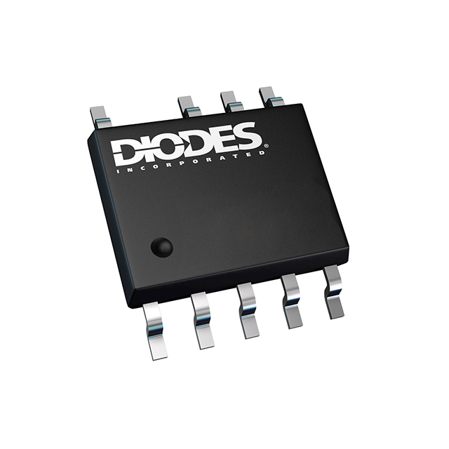
Diodes Incorporated AP3118GSTR-G1
- Part No.:
- AP3118GSTR-G1
- Manufacturer:
- Diodes Incorporated
- Category:
- DC DC Switching Controllers
- Package:
- 10-SOP (0.154", 3.90mm Width), 9 Leads
- Datasheet:
-
 AP3118GSTR-G1.pdf
- Description:
- ACDC SINGLE ENDED CONT SSOP-9
- Quantity:
- Payment:

- Shipping:

Inventory:2,392
Please send an inquiry. Send us your inquiry, and we will respond immediately.
Product details
Overview
AP3118GSTR-G1 from Diodes Incorporated is a current-mode multi-mode PWM controller for offline AC-DC power supplies, featuring 65 kHz fixed-frequency operation, green-mode frequency foldback (20–30 kHz), peak-load boost to 120 kHz, integrated HV startup (700 V max), and X-CAP discharge functionality. It delivers ultra-low standby power in USB PD adapter and open-frame SMPS designs.
For engineers reviewing the AP3118GSTR-G1 datasheet, AP3118GSTR-G1 pinout, AP3118GSTR-G1 application, or AP3118GSTR-G1 equivalent, key selection criteria include its dual-threshold brownout detection (100/97 V), precise secondary-side OVP/UVP (±1.1% reference), programmable external OTP, and burst-mode entry at 0.66 V FB with 130 mV hysteresis.
Technical Context
The AP3118 implements adaptive frequency control: fixed 65 kHz under heavy load, smooth reduction to 25 kHz in green mode to avoid audible noise, and transient boost to 120 kHz for up to 30 ms during peak load. Its internal slope compensation and 250 ns leading-edge blanking ensure stable cycle-by-cycle current limiting across line and load variations.
It integrates a wide-input LDO (10–60 V VCC_IN) regulating to 9.8–16 V VCC, a high-voltage startup circuit with three charge-current modes (0.23 mA / 1.8 mA / 90 µA), and a dedicated DEM pin for de-magnetization sensing enabling precise SOVP/SUVP protection with 75 mV threshold and 7-cycle debounce.
Key Specifications
| Parameter | Value and Actual Design Meaning |
|---|---|
| Switching Frequency | 65 kHz nominal; 20–30 kHz green mode; 110–130 kHz peak mode - enables high efficiency across load range while avoiding audible noise |
| VCC UVLO Threshold | 6.1–7.1 V - ensures reliable startup and shutdown with 0.4 V hysteresis for stable brownout recovery |
| FB Input Impedance | 19–31 kΩ - supports standard optocoupler feedback networks without loading error |
| SENSE Reference Voltage | 2.45–2.55 V - provides accurate primary current sensing for constant-output-current regulation |
| HV Pin Max Voltage | 700 V - enables direct connection to rectified AC line for simplified high-voltage startup |
| X-CAP Discharge Current | 1.3–2.1 mA - replaces external bleed resistors, reducing standby power by >100 mW in typical 100 nF X-CAP designs |
| Gate Drive Output | 100 mA sink/source, 150 ns rise/50 ns fall - drives 1 Ω gate resistance MOSFETs directly in <100 W adapters |
Pinout & Package
AP3118GSTR-G1 is housed in an SSOP-9 (Type CJ) package with exposed thermal pad, RoHS-compliant, halogen-free, and lead-free construction.
| Pin/Terminal | Circuit Role | Design Meaning |
|---|---|---|
| 1 CTRL | Programmable External Protection Input | Accepts external fault signal (0.96–3.15 V thresholds); triggers latch-off or hiccup on overtemperature or system faults |
| 2 FB | Feedback Input | Receives optocoupler output; controls duty cycle via error amplifier; burst mode triggered below 0.66 V |
| 3 DEM | De-magnetization Sense | Detects transformer reset; enables accurate secondary-side OVP (4.5 V) and UVP (0.5 V) with 75 mV threshold |
| 4 VCC_IN | LDO Input Supply | Wide-range input (10–60 V); powers internal LDO to generate regulated 9.8–16 V VCC supply |
| 5 GND | Signal Ground Reference | Common return for all analog and digital circuits; isolated from power ground in layout-critical designs |
| 6 GATE | High-Side MOSFET Driver Output | 100 mA capable driver; 1 V low-level / 6.4 V high-level at 15 mA; clamped at 10.5 V |
| 7 VCC | Internal Regulated Supply | Output of integrated LDO; powers control logic and gate driver; monitored for OVP (33 V) and UVLO (6.7 V) |
| 8 SENSE | Primary Current Sense Input | Monitors RCS voltage; includes 250 ns LEB and 2.5 V reference for cycle-by-cycle OCP and constant-current regulation |
| 9 HV | High-Voltage Startup & Line Sense | 700 V rated input; provides startup current (0.23 mA @ VCC=0); senses AC line for X-CAP discharge and brown-in/out |
Key Features
| Feature | Design Value |
|---|---|
| Green-mode frequency foldback | Smoothly reduces switching frequency from 65 kHz to 25 kHz as load decreases - improves light-load efficiency by >8% vs fixed-frequency operation |
| Integrated X-CAP discharge | 1.7 mA typical discharge current - eliminates need for 1 MΩ/1 W bleed resistors, cutting standby loss by ~120 mW in 65 W adapters |
| Constant output current limit | Uses mid-point current sampling + line-compensated calculation - maintains ±5% output current accuracy across 90–264 VAC input |
| VCC LDO with wide input range | Regulates 10–60 V VCC_IN to stable 9.8–16 V VCC - enables single-supply auxiliary winding design without external regulator |
| Audible-noise suppression | Minimum 25 kHz switching frequency + ±6% dithering - avoids 20–20 kHz audio band and reduces EMI peak amplitude by 10 dB |
Applications
| USB PD Adapters | Open-Frame SMPS |
|---|---|
|
Use Scenario: 20–65 W USB-C power adapters with programmable voltage/current profiles. IC Role / Device Role / Timing Role: Primary-side PWM controller coordinating with secondary USB PD IC via optocoupler feedback; manages green mode, burst mode, and peak-load frequency boost. Use Value: Enables <30 mW no-load standby power and <89% average efficiency across 10–100% load per DOE VI/CoC Tier 2 requirements. |
Use Scenario: Industrial/open-frame 36–75 W AC-DC power supplies for IoT gateways and PoE injectors. IC Role / Device Role / Timing Role: Core PWM controller with HV startup and X-CAP discharge - simplifies front-end design and eliminates external discharge resistors. Use Value: Reduces BOM count by 2–3 components and cuts no-load dissipation by 150 mW versus discrete HV start solutions. |
| Universal Input Adapters | USB-C Wall Chargers |
|
Use Scenario: Dual-port 30 W universal-input (90–264 VAC) travel adapters with foldable plug. IC Role / Device Role / Timing Role: Multi-mode controller implementing burst mode at <5% load, green mode at 10–40%, and peak mode for transient 150% overload. Use Value: Achieves <25 mW standby and passes IEC 62368-1 touch-current limits due to integrated X-CAP discharge and low ICC (0.45 mA). |
Use Scenario: Compact 45 W wall-mounted USB-C chargers with high-power density (>15 W/in³). IC Role / Device Role / Timing Role: High-efficiency PWM controller using frequency dithering and soft-start to meet CISPR-32 Class B conducted EMI limits. Use Value: Passes EMI without Y-capacitor doubling; reduces heatsink size by 30% via 150°C OTP with 25°C hysteresis. |
Equivalent & Alternatives
The following parts are listed as comparable options for similar multi-mode PWM controller applications.
| Alternative Part | Technical Difference | Application Difference | Selection Advice |
|---|---|---|---|
| ON Semiconductor NCP1342 | Fixed 65 kHz + valley-switching; no HV pin; requires external startup resistor; lacks X-CAP discharge | Requires additional HV startup network and bleed resistors; higher standby power in no-load condition | Preferred when cost-sensitive designs accept added BOM and 50 mW higher standby |
| Infineon ICE2QS03G | Quasi-resonant only; no green/burst modes; 12 V VCC UVLO; no integrated LDO for wide VCC_IN | Cannot support universal input without auxiliary winding regulation; no X-CAP discharge or line-sense brownout | Only suitable for fixed-input, non-USB-PD applications where QR efficiency suffices |
Compared with NCP1342 and ICE2QS03G, the AP3118GSTR-G1 uniquely integrates HV startup, X-CAP discharge, and multi-mode frequency control - delivering lowest BOM count and <30 mW standby in universal-input USB PD systems, but requires careful layout for HV pin noise immunity.
Availability
AP3118GSTR-G1 is available at Aetrix Electronics and suitable for USB PD adapters, open-frame SMPS, universal-input chargers, and compact wall-mount power supplies requiring stable component supply and long-term lifecycle support.
Supply support for AP3118GSTR-G1 includes scheduled delivery planning, volume procurement assistance, BOM continuity management, traceable sourcing, and lifecycle availability coordination for OEM customers, industrial embedded developers, connected-device designers, and electronics production programs.
Manufacturer
Diodes Incorporated is a global manufacturer of discrete semiconductors and analog ICs, headquartered in Plano, Texas, with design centers across Asia and manufacturing in IATF 16949-certified facilities.
The AP3118 belongs to Diodes' high-efficiency AC-DC controller product line, designed specifically for ultra-low-standby, multi-mode offline power conversion in USB PD and energy-efficient consumer adapters.
FAQ
What is the purpose of the HV pin on the AP3118GSTR-G1?
The HV pin serves two critical functions: it provides high-voltage startup current (0.23 mA at VCC = 0 V) directly from the rectified AC line to charge the VCC capacitor, eliminating external startup resistors; and it senses line voltage to enable automatic X-CAP discharge when AC power is removed, replacing external bleed resistors and reducing standby power by up to 120 mW.
How does the AP3118GSTR-G1 achieve constant output current during short-circuit conditions?
The AP3118 uses mid-point primary current sampling (VCSM) combined with line-voltage-compensated timing to maintain constant output current. It calculates Io = VREF / RCS × NP/NS × KCC (KCC = 1/8), where VREF is tightly regulated at 2.5 V ±2%. This method holds output short-circuit current within ±5% across 90–264 VAC input, independent of transformer turns ratio or sense resistor tolerance.
Can the AP3118GSTR-G1 operate without an auxiliary winding?
No - the AP3118 requires an auxiliary winding to sustain VCC after startup. The HV pin only provides initial charge current until VCC reaches 14.8 V; thereafter, the auxiliary winding supplies VCC via the integrated LDO. Without it, the IC will repeatedly enter UVLO shutdown after startup, causing unstable burst-mode oscillation and potential thermal stress.
What protection features are implemented on the DEM pin?
The DEM pin enables secondary-side overvoltage protection (SOVP) and undervoltage protection (SUVP) by detecting transformer demagnetization timing. It triggers SOVP at 4.5 V (steady-state) or 1.1 V (startup) with 7-cycle debounce, and SUVP at 0.5 V with 27 ms blank time post-startup. These protections act independently of optocoupler latency, providing <10 µs response to output overvoltage events.
AP3118GSTR-G1 Specifications
- Product attributes
- Attribute value
- Manufacturer:
- Diodes Incorporated
- Series:
- -
- Package/Case:
- 10-SOP (0.154", 3.90mm Width), 9 Leads
- Packaging:
- Tape & Reel (TR)
- Product Status:
- Active
- Output Type:
- PWM
- Function:
- Step-Down
- Output Configuration:
- Positive
- Topology:
- -
- Number of Outputs:
- 1
- Output Phases:
- 1
- Voltage - Supply (Vcc/Vdd):
- 10V ~ 28V
- Frequency - Switching:
- 120kHz
- Duty Cycle (Max):
- 80%
- Synchronous Rectifier:
- No
- Clock Sync:
- No
- Serial Interfaces:
- -
- Control Features:
- -
- Operating Temperature:
- -40°C ~ 85°C (TA)
- Grade:
- -
- Qualification:
- -
- Mounting Type:
- Surface Mount
- Supplier Device Package:
- 9-SSOP
AP3118GSTR-G1 FAQ
1.How can I place an order for AP3118GSTR-G1 through Aetrix?
Please submit a Request for Quotation (RFQ) for AP3118GSTR-G1 on Aetrix. Our sales agent will provide a competitive quotation and guide you through the order confirmation once you accept the terms.
2.Are the price and stock information for AP3118GSTR-G1 reliable?
The price and inventory of AP3118GSTR-G1 are updated periodically and may fluctuate due to market conditions. Stock and pricing data are typically refreshed every 24 hours. Quotation validity for AP3118GSTR-G1 is usually 5 days.
3.What payment methods are accepted for AP3118GSTR-G1?
We accept Wire Transfer, PayPal, Credit Card, Western Union, MoneyGram, and Escrow for AP3118GSTR-G1 transactions.
Note: Certain payment methods may incur a processing fee.
4.How is shipping managed for AP3118GSTR-G1?
AP3118GSTR-G1 orders can be shipped via leading logistics carriers, including DHL, UPS, FedEx, TNT, or Registered Mail.
Once your AP3118GSTR-G1 order is processed, you will receive an email with the shipment details and tracking number.
Note: Tracking information may take up to 24 hours to appear. Express delivery typically takes 3–5 business days.
5.How can I obtain technical support or documentation for AP3118GSTR-G1?
For technical support, including AP3118GSTR-G1 datasheets, pinout diagrams, or application guidance, please contact our engineering support team. They can provide detailed documentation and assistance for your AP3118GSTR-G1 requirements.
6.How does Aetrix verify that AP3118GSTR-G1 is sourced from the original manufacturer or authorized distributors?
All AP3118GSTR-G1 products on Aetrix are procured from qualified distributors and authorized channels. Our dedicated quality assurance team conducts strict verification, including traceability checks and, if necessary, third-party testing. This ensures that AP3118GSTR-G1 meets industry standards.
7.What is the process for return or replacement of AP3118GSTR-G1?
All AP3118GSTR-G1 units undergo pre-shipment inspection (PSI). If there is an issue with AP3118GSTR-G1, returns or replacements are accepted under the following conditions:
1.Quantity discrepancies, incorrect items, or visible external defects (such as breakage or corrosion), acknowledged by Aetrix.
2.The issue is reported within 90 days of delivery.
3.The AP3118GSTR-G1 part is unused and in its original packaging.
Return procedure for AP3118GSTR-G1:
1.Submit a request within 90 days.
2.Obtain a Return Material Authorization (RMA) from Aetrix.
AP3118GSTR-G1 Tags

-
UCC28C45DR
Texas Instruments
-
UCC28C40DR
Texas Instruments
-
UCC28C43DR
Texas Instruments

-
ZXSC410E6TA
Diodes Incorporated

-
LM3524DMX/NOPB
Texas Instruments

-
LM3489MMX/NOPB
Texas Instruments
-
MIC2102YML-TR
Microchip Technology

-
LM5148RGYR
Texas Instruments
-
TL598CDR
Texas Instruments

-
LM5155DSSR
Texas Instruments

-
LM25085MYX/NOPB
Texas Instruments
-
UCC2813DTR-0
Texas Instruments
Tech Hub

Operational amplifier guide covering op amp basics, feedback, ideal vs real op amps, common configurations, buffer circuits, offset, bias current, gain-bandwidth, slew rate, rail-to-rail limits and sel…

Jumper cables guide covering safe connection order, red and black clamp placement, final ground connection, cable gauge, length, clamp quality, copper vs CCA cables, jump starter comparison and battery…

LDO regulator guide covering low dropout voltage, power dissipation, thermal design, PSRR, output noise, capacitor stability, adjustable LDO circuits, LDO vs buck converter and datasheet selection chec…

Conditional Access Module guide covering CAM meaning, CI/CI+ interface, smart card authorization, DVB security workflow, TV and set-top box compatibility, internal electronics, ESD protection, connecto…

Guide to electronic component obsolescence covering EOL risk, PCN/PDN notices, last-time buy planning, replacement options, form-fit-function validation, counterfeit risk and BOM lifecycle management.

18650 battery guide covering lithium-ion cell basics, 3.6V/3.7V voltage, 4.2V charging, mAh and Wh capacity, protected cells, chargers, BMS, series-parallel packs, holders, welding and sourcing checks.…

Hall effect sensor guide covering working principle, linear and digital sensors, Arduino circuits, current sensing, speed detection, automotive applications, A3144 examples, signal filtering and datash…

Product Change Notification guide for electronic components, covering PCN meaning, PCN vs PDN/EOL, common change types, risk levels, form-fit-function review, engineering validation, BOM control, LTB/L…

A practical guide to blend door actuators, covering HVAC function, symptoms, location, AC and heater issues, reset and calibration, replacement cost, electrical diagnosis, compatibility checks, and rep…

Engineering guide to Raspberry Pi alternatives, covering chip-level differences, Orange Pi, ROCK, Jetson, Banana Pi, NanoPi, Compute Module, Pico, GPIO, camera, HAT compatibility, and replacement risks…


