
 My Inquiry
 My Account


Diodes Incorporated AP3306S10-13
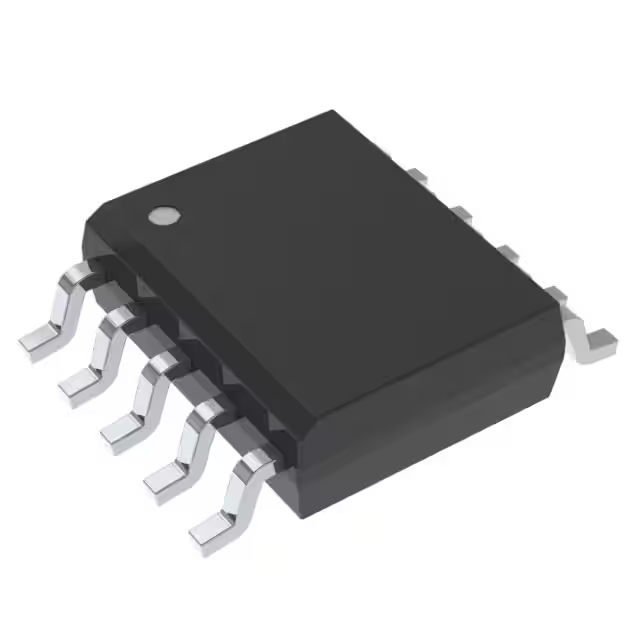
- Part No.:
- AP3306S10-13
- Manufacturer:
- Diodes Incorporated
- Category:
- AC DC Converters, Offline Switches
- Package:
- 10-SOP (0.154", 3.90mm Width)
- Datasheet:
-
 AP3306S10-13.pdf
- Description:
- ACDC PWM SWITCHER SO-10 T&R 2.5K
- Quantity:
- Payment:

- Shipping:

Inventory:2,144
Please send an inquiry. Send us your inquiry, and we will respond immediately.
Product details
Overview
AP3306S10-13 from Diodes Incorporated is a highly integrated Active Clamp Flyback (ACF) PWM controller for offline AC-DC power supplies, featuring 22–125 kHz switching frequency range, 0.56 V current sense threshold, ±3% frequency dithering, built-in X-CAP discharge, and SO-10 (Type A1) package. It enables ultra-low standby power (<0.33 mA burst mode), ZVS operation, and wide-output-voltage support for USB-PD 3.0 PPS chargers.
For engineers reviewing the AP3306S10-13 datasheet, AP3306S10-13 pinout, AP3306S10-13 application, or AP3306S10-13 equivalent, key selection criteria include active clamp control logic, dual gate drivers (GDH/GDL) for high-side PMOS and low-side NMOS, VCCL LDO regulation (10–50 V input), HV startup capability (700 V max), and secondary-side OVP/UVP protection with DEM pin sampling.
Technical Context
The AP3306 implements a patented Smart Active Clamp Control Strategy combining valley switching and jittered ZVS to recycle leakage energy and minimize switching loss across universal input (90–264 VAC). Its dual-mode operation-valley-switching at low line/full load and ZVS-with-jitter at high line-ensures consistent efficiency and EMI compliance without external compensation.
It integrates a dedicated HV startup circuit with fault-aware charge current (ICHARGE-L/ICHARGE-H/ICHARGE-FAULT), a VCCH-to-VCCL LDO enabling 10–50 V VCCL operation, and a DEM pin that performs simultaneous functions: demagnetization detection, SOVP/SUVP sampling (with 1.8 µs delay), and OCP line compensation-enabling single-pin secondary-side monitoring.
Key Specifications
| Parameter | Value and Actual Design Meaning |
|---|---|
| Topology | Active Clamp Flyback (ACF) with pseudo-ZVS and leakage energy recycling |
| Switching Frequency Range | 22–125 kHz (non-jitter); ±3% dithering reduces EMI peak emissions |
| Current Sense Threshold | 0.56 V typical; sets primary peak current limit via CS pin resistor |
| VCC LDO Input Range | VCCH = 8.5–120 V; regulates VCCL to stable 5–6 V for internal logic and gate drivers |
| Gate Drive Outputs | GDH (PMOS high-side, 0.8 V low / 7 V high w.r.t. VCCL) and GDL (NMOS low-side, 0.8 V low / 7 V high w.r.t. GND) |
| Protection Features | Brown-out (VBR-IN = 102 V), SOVP (3.2 V), SUVP (0.4 V), VOVP (55 V), OTP (+150 °C), FOCP (1.2 V), X-CAP discharge (1.7 mA) |
| Startup Mechanism | HV pin supports 700 V max input; provides ICHARGE-L/H/FAULT currents for reliable cold-start and fault-recovery |
Pinout & Package
AP3306S10-13 is housed in a SO-10 (Type A1) surface-mount package with exposed thermal pad (JEDEC MS-012 variant), 1.75 mm max height, and matte tin annealed lead finish compliant with J-STD-020 Level 3 moisture sensitivity.
| Pin/Terminal | Circuit Role | Design Meaning |
|---|---|---|
| VCCH (Pin 1) | LDO input supply | Accepts 8.5–120 V wide-range auxiliary winding voltage; powers internal LDO to regulate VCCL |
| FB (Pin 2) | Optocoupler feedback input | Sets output voltage via resistive divider; triggers burst mode below 0.6 V and green mode modulation |
| DEM (Pin 3) | Demagnetization & protection monitor | Detects transformer reset timing, samples secondary voltage for SOVP/SUVP, and compensates OCP for line variation |
| VCCL (Pin 4) | Internal logic & driver supply | Regulated 5–6 V output of VCCH LDO; powers control circuitry and gate drivers (10–50 V operational range) |
| GDH (Pin 5) | High-side PMOS gate driver | Pulls down to turn on PMOS (source tied to VCCL); pulls up to VCCL to turn off; supports 300 mA sink/source |
| GDL (Pin 6) | Low-side NMOS gate driver | Drives NMOS switch with 800 mA sink capability; logic-level compatible with GND-referenced gate |
| GND (Pin 7) | Signal ground reference | Common return path for CS, FB, DEM, GDH, GDL, and internal analog/digital blocks |
| CS (Pin 8) | Primary current sense input | Monitors primary-side current via shunt resistor; triggers FOCP at 1.2 V and cycle-by-cycle OCP at 0.56 V |
| NC (Pin 9) | No connect | Internally unconnected; must remain floating per design; no external connection permitted |
| HV (Pin 10) | High-voltage line sensing & startup | Detects AC line presence (92–112 V brown-in), enables X-CAP discharge, and delivers startup current to VCCL |
Key Features
| Feature | Design Value |
|---|---|
| Smart Active Clamp Control | Valley-switching + jittered ZVS enables >94% efficiency at 30W/in³ density while reducing MOSFET stress |
| Integrated X-CAP Discharge | 1.7 mA HV-pin discharge current replaces external bleeder resistors, cutting standby power by ~30 mW |
| VCCL LDO Regulation | Accepts 10–50 V VCCL input and maintains stable rail for gate drivers-critical for variable-output USB-PD designs |
| Multi-Stage Protection Architecture | FOCP (7-cycle response), SOVP/SUVP (sampled via DEM), BNO, VOVP, OTP, and pin-fault detection ensure robust field reliability |
| Non-Audible Burst Mode | Minimum 22 kHz switching frequency prevents acoustic noise; 0.33 mA operating current enables <30 mW no-load consumption |
Applications
| Smartphone Quick Chargers | Notebook Adapters |
|---|---|
|
Use Scenario: 30–65 W USB-PD 3.0 PPS charger with 3.3–21 V output range and <30 mW no-load power. IC Role / Device Role / Timing Role: Primary-side ACF controller managing high-side PMOS and low-side NMOS switching, ZVS timing, and opto-coupler feedback loop. Use Value: Enables compact 30 W/in³ power density and meets DOE VI/ERP Tier 2 standby requirements via burst mode and X-CAP discharge. |
Use Scenario: 65–100 W slim-profile notebook adapter supporting 20 V @ 5 A with dynamic voltage scaling. IC Role / Device Role / Timing Role: Core ACF PWM controller coordinating GDH/GDL gate timing, DEM-based SOVP, and VCCL LDO for wide-output regulation. Use Value: Delivers >93% average efficiency across 10–100% load with frequency foldback and eliminates audible noise via 22 kHz minimum frequency. |
| ATX/BTX Auxiliary Power | Open-Frame SMPS |
|
Use Scenario: 5–12 V/3 A auxiliary rail in ATX PSUs requiring <100 mW no-load draw and high surge immunity. IC Role / Device Role / Timing Role: Standalone ACF controller providing isolated 5 V/12 V outputs with brown-in/out protection and HV-line sensing. Use Value: Replaces discrete startup circuits and external OVP comparators-reducing BOM count by ≥4 components. |
Use Scenario: Industrial open-frame 24–48 V/5 A power supply with safety-critical OVP/UVP and thermal shutdown. IC Role / Device Role / Timing Role: Primary-side controller executing ZVS timing, OTP-triggered latch-off, and DEM-sampled secondary protection. Use Value: Achieves Class II isolation compliance and eliminates need for secondary-side protection ICs via integrated SOVP/SUVP. |
Equivalent & Alternatives
The following parts are listed as comparable options for similar active clamp flyback controller applications.
| Alternative Part | Technical Difference | Application Difference | Selection Advice |
|---|---|---|---|
| ON Semiconductor NCP1566 | Fixed 100 kHz max frequency; no VCCL LDO; requires external VCC regulator; lacks X-CAP discharge | Targeted at fixed-output 12–19 V adapters; not optimized for USB-PD variable voltage | Select when cost-sensitive fixed-output designs prioritize simplicity over ultra-low standby |
| Power Integrations INN3377C | Integrated high-voltage switch (750 V); no GDH/GDL pins; uses digital control; higher BOM cost | Designed for fully integrated InnoSwitch3-based solutions; no external MOSFETs required | Choose for highest integration level and reduced layout complexity, accepting higher unit cost |
Compared with NCP1566 and INN3377C, the AP3306S10-13 uniquely combines wide VCCL regulation (10–50 V), dual gate drivers, and X-CAP discharge-making it optimal for high-density, variable-output USB-PD chargers where standby power, board space, and secondary-side protection integration are critical.
Availability
AP3306S10-13 is available at Aetrix Electronics and suitable for smartphone quick chargers, notebook computer adapters, and open-frame switching power supplies requiring stable component supply, long-term lifecycle support, and RoHS-compliant manufacturing.
Supply support for AP3306S10-13 includes scheduled delivery planning, volume procurement assistance, BOM continuity management, traceable sourcing, and lifecycle availability coordination for OEM customers, industrial embedded developers, connected-device designers, and electronics production programs.
Manufacturer
Diodes Incorporated is a global manufacturer of discrete semiconductors and ICs, specializing in power management, signal integrity, and protection solutions for consumer, industrial, and computing markets.
The AP3306 belongs to Diodes' Active Clamp Flyback Controller product line, engineered specifically for high-efficiency, high-power-density offline AC-DC converters targeting USB-PD, QC, and other programmable power supply standards.
FAQ
What is the purpose of the DEM pin in AP3306S10-13?
The DEM pin serves three concurrent functions: detecting transformer demagnetization timing to enable ZVS, sampling auxiliary winding voltage for secondary-side OVP (3.2 V threshold) and UVP (0.4 V threshold), and providing line-voltage-compensated current sense for accurate OCP across input range. It operates with a fixed 1.8 µs sample delay after GATE falling edge.
How does the HV pin support both startup and X-CAP discharge?
The HV pin senses AC line voltage for brown-in/out protection and provides startup current to VCCL until VST (15.8 V) is reached. When AC is removed, an internal 40 ms timer detects disconnection and activates a 1.7 mA discharge current through HV→GND for 40 ms, repeating until HV voltage falls below 10 V-eliminating need for external bleeder resistors.
Can AP3306S10-13 drive both high-side PMOS and low-side NMOS simultaneously?
Yes-GDH drives the gate of a high-side PMOS (source tied to VCCL) by pulling down to turn on and pulling up to VCCL to turn off; GDL drives a low-side NMOS (source tied to GND) with standard logic-level output. Both drivers operate with matched timing and support independent dead-time control via internal logic.
What protection features trigger automatic restart versus latched shutdown?
All protections-including BNO, FOCP, SOVP, SUVP, VOVP, OTP, and OCP-cause immediate shutdown and automatic restart once VCCL falls below UVLO (6.5 V). No latched modes exist; recovery is fully autonomous, relying on VCC decay/recharge cycle, ensuring robustness in intermittent fault conditions like line sags or transient shorts.
AP3306S10-13 Specifications
- Product attributes
- Attribute value
- Manufacturer:
- Diodes Incorporated
- Series:
- -
- Package/Case:
- 10-SOP (0.154", 3.90mm Width)
- Packaging:
- Tape & Reel (TR)
- Product Status:
- Active
- Output Isolation:
- Isolated
- Internal Switch(s):
- No
- Voltage - Breakdown:
- 700V
- Topology:
- Flyback
- Voltage - Start Up:
- 15.8 V
- Voltage - Supply (Vcc/Vdd):
- 10V ~ 50V
- Duty Cycle:
- -
- Frequency - Switching:
- 130kHz, 200kHz
- Power (Watts):
- -
- Fault Protection:
- Current Limiting, Over Load, Over Temperature, Over Voltage
- Control Features:
- Soft Start
- Operating Temperature:
- -40°C ~ 85°C (TA)
- Grade:
- Automotive
- Qualification:
- AEC-Q100
- Supplier Device Package:
- 10-SO Type A1
- Mounting Type:
- Surface Mount
AP3306S10-13 FAQ
1.How can I place an order for AP3306S10-13 through Aetrix?
Please submit a Request for Quotation (RFQ) for AP3306S10-13 on Aetrix. Our sales agent will provide a competitive quotation and guide you through the order confirmation once you accept the terms.
2.Are the price and stock information for AP3306S10-13 reliable?
The price and inventory of AP3306S10-13 are updated periodically and may fluctuate due to market conditions. Stock and pricing data are typically refreshed every 24 hours. Quotation validity for AP3306S10-13 is usually 5 days.
3.What payment methods are accepted for AP3306S10-13?
We accept Wire Transfer, PayPal, Credit Card, Western Union, MoneyGram, and Escrow for AP3306S10-13 transactions.
Note: Certain payment methods may incur a processing fee.
4.How is shipping managed for AP3306S10-13?
AP3306S10-13 orders can be shipped via leading logistics carriers, including DHL, UPS, FedEx, TNT, or Registered Mail.
Once your AP3306S10-13 order is processed, you will receive an email with the shipment details and tracking number.
Note: Tracking information may take up to 24 hours to appear. Express delivery typically takes 3–5 business days.
5.How can I obtain technical support or documentation for AP3306S10-13?
For technical support, including AP3306S10-13 datasheets, pinout diagrams, or application guidance, please contact our engineering support team. They can provide detailed documentation and assistance for your AP3306S10-13 requirements.
6.How does Aetrix verify that AP3306S10-13 is sourced from the original manufacturer or authorized distributors?
All AP3306S10-13 products on Aetrix are procured from qualified distributors and authorized channels. Our dedicated quality assurance team conducts strict verification, including traceability checks and, if necessary, third-party testing. This ensures that AP3306S10-13 meets industry standards.
7.What is the process for return or replacement of AP3306S10-13?
All AP3306S10-13 units undergo pre-shipment inspection (PSI). If there is an issue with AP3306S10-13, returns or replacements are accepted under the following conditions:
1.Quantity discrepancies, incorrect items, or visible external defects (such as breakage or corrosion), acknowledged by Aetrix.
2.The issue is reported within 90 days of delivery.
3.The AP3306S10-13 part is unused and in its original packaging.
Return procedure for AP3306S10-13:
1.Submit a request within 90 days.
2.Obtain a Return Material Authorization (RMA) from Aetrix.
AP3306S10-13 Tags
-
LNK6407D-TL
Power Integrations
-
LNK3204D-TL
Power Integrations

-
SR10LG-G
Microchip Technology
-
TNY285DG-TL
Power Integrations
-
LNK304DN-TL
Power Integrations
-
TNY285KG-TL
Power Integrations
-
LNK3206D-TL
Power Integrations
-
LNK623DG-TL
Power Integrations
-
TNY286PG
Power Integrations
-
LNK624DG-TL
Power Integrations
-
LNK604DG-TL
Power Integrations

-
UCC28704DBVR-1
Texas Instruments
Tech Hub

Operational amplifier guide covering op amp basics, feedback, ideal vs real op amps, common configurations, buffer circuits, offset, bias current, gain-bandwidth, slew rate, rail-to-rail limits and sel…

Jumper cables guide covering safe connection order, red and black clamp placement, final ground connection, cable gauge, length, clamp quality, copper vs CCA cables, jump starter comparison and battery…

LDO regulator guide covering low dropout voltage, power dissipation, thermal design, PSRR, output noise, capacitor stability, adjustable LDO circuits, LDO vs buck converter and datasheet selection chec…

Conditional Access Module guide covering CAM meaning, CI/CI+ interface, smart card authorization, DVB security workflow, TV and set-top box compatibility, internal electronics, ESD protection, connecto…

Guide to electronic component obsolescence covering EOL risk, PCN/PDN notices, last-time buy planning, replacement options, form-fit-function validation, counterfeit risk and BOM lifecycle management.

18650 battery guide covering lithium-ion cell basics, 3.6V/3.7V voltage, 4.2V charging, mAh and Wh capacity, protected cells, chargers, BMS, series-parallel packs, holders, welding and sourcing checks.…

Hall effect sensor guide covering working principle, linear and digital sensors, Arduino circuits, current sensing, speed detection, automotive applications, A3144 examples, signal filtering and datash…

Product Change Notification guide for electronic components, covering PCN meaning, PCN vs PDN/EOL, common change types, risk levels, form-fit-function review, engineering validation, BOM control, LTB/L…

A practical guide to blend door actuators, covering HVAC function, symptoms, location, AC and heater issues, reset and calibration, replacement cost, electrical diagnosis, compatibility checks, and rep…

Engineering guide to Raspberry Pi alternatives, covering chip-level differences, Orange Pi, ROCK, Jetson, Banana Pi, NanoPi, Compute Module, Pico, GPIO, camera, HAT compatibility, and replacement risks…


