
 My Inquiry
 My Account


Diodes Incorporated AP3591FNTR-G1
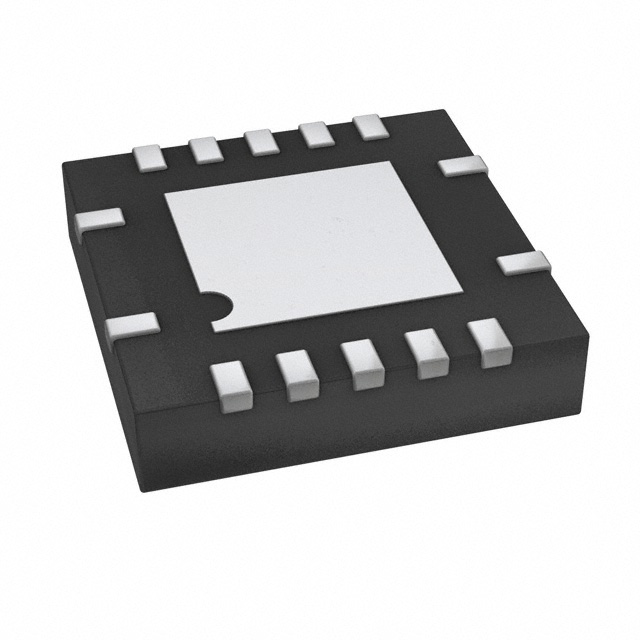
- Part No.:
- AP3591FNTR-G1
- Manufacturer:
- Diodes Incorporated
- Category:
- DC DC Switching Controllers
- Package:
- 14-VFQFN Exposed Pad
- Datasheet:
-
 AP3591FNTR-G1.pdf
- Description:
- IC REG CTRLR BUCK U-QFN3535-14
- Quantity:
- Payment:

- Shipping:

Inventory:2,607
Please send an inquiry. Send us your inquiry, and we will respond immediately.
Product details
Overview
AP3591FNTR-G1 from Diodes Incorporated is a single-phase synchronous buck controller implementing adaptive constant-on-time (COT) PWM control for notebook and low-voltage distributed power applications. It delivers 0.75V–5.5V output with ±1% feedback reference accuracy (0.742–0.758V), supports 4.5V–26V input, and features integrated DEM/CCM mode selection via EN/DEM pin voltage, internal soft-start (1.2ms typical), and power-good monitoring with ±5% threshold hysteresis.
For engineers reviewing the AP3591FNTR-G1 datasheet, AP3591FNTR-G1 pinout, AP3591FNTR-G1 application, or AP3591FNTR-G1 equivalent, key selection criteria include its resistor-programmable switching frequency (100–700kHz), RDS(ON)-based current sensing with 4500ppm/°C temperature compensation, integrated bootstrap diode, safe pre-biased start-up, and dual over-current protection (positive/negative) with programmable trip point.
Technical Context
The AP3591FNTR-G1 uses adaptive COT control without an external clock, deriving on-time from VOUT/VIN ratio and RTON, enabling stable operation across wide input-output voltage ratios. Its error amplifier compares FB to a 0.75V reference, and internal soft-start ramps VSS to 95% of reference in 1.2ms to limit inrush current.
Mode selection is voltage-defined: EN/DEM ≥2.9V enables Diode Emulation Mode (light-load efficiency), floating EN/DEM forces Continuous Conduction Mode (constant-frequency noise control), and EN/DEM ≤1.6V disables operation. Protection includes UVLO (3.9V VDD threshold), OTP (160°C shutdown), OVP/UVP (125%/70% VFB thresholds), and cycle-by-cycle NOCP with 400ns recovery delay.
Key Specifications
| Parameter | Value and Actual Design Meaning |
|---|---|
| Control Method | Adaptive constant-on-time (COT); enables fast transient response and eliminates need for loop compensation components. |
| Input Voltage Range | 4.5V to 26V; supports wide-range DC inputs including 5V, 12V, and 19V adapter rails in portable systems. |
| Output Voltage Range | 0.75V to 5.5V; set via resistor divider on FB pin with 0.75V ±10mV reference for precise core/I/O rail regulation. |
| Switching Frequency | 100kHz to 700kHz; resistor-programmable via TON pin, enabling optimization of size vs. efficiency vs. EMI. |
| Current Sensing | RDS(ON)-based low-side sensing with 10µA CS current source and 4500ppm/°C tempco; compensates MOSFET resistance drift for stable OCP across temperature. |
| Protection Features | Integrated UVLO (3.9V), OVP (125% VFB), UVP (70% VFB), OTP (160°C), and dual OCP (positive/negative) with programmable trip via CS-to-GND resistor. |
| Power Good | Open-drain PGOOD with ±5% threshold hysteresis and 22µs typical delay; signals valid regulation after soft-start completion. |
Pinout & Package
AP3591FNTR-G1 is housed in a thermally enhanced U-QFN3535-14 package (3.5mm × 3.5mm, 0.5mm pitch) with exposed thermal pad soldered to PCB ground for optimal power dissipation (θJA = 60°C/W).
| Pin | Circuit Role | Design Meaning |
|---|---|---|
| 1 EN/DEM | Enable / Diode Emulation Mode control | Voltage-selectable mode: ≥2.9V → DEM (efficiency), float → CCM (noise control), ≤1.6V → shutdown. |
| 2 TON | On-time / Frequency adjustment | Resistor-connected node setting switching frequency from 100–700kHz; determines tON per COT equation. |
| 3 VOUT | Output voltage sense return | Direct connection to converter output; used internally for adaptive on-time calculation and soft-stop discharge path. |
| 4 VDD | Analog supply input | 4.5–5.5V bias for internal analog circuitry; requires 1µF ceramic bypass to GND for stability. |
| 5 FB | Feedback input | Monitors output via resistor divider; 0.75V reference enables accurate VOUT regulation from 0.75V to 5.5V. |
| 6 PGOOD | Power good open-drain output | Signals regulation status with ±5% window; pulled high only after soft-start and within tolerance for ≥22µs. |
| 7 GND | Analog ground reference | Reference for all analog functions; separate from PGND to minimize noise coupling into feedback path. |
| 8 PGND | Power ground return | High-current return path for gate drivers and MOSFET sources; tied to GND externally but isolated internally. |
| 9 LGATE | Low-side N-MOSFET gate driver | Drives LS-FET gate between PGND and VDDP; sink/source capability ensures fast turn-on/turn-off transitions. |
| 10 VDDP | Gate driver supply | 5V supply for UGATE/LGATE drivers; bypassed with 1µF ceramic capacitor to PGND for low-impedance drive. |
| 11 CS | Current sense threshold set | Connects to GND via resistor to program OCP trip point; 10µA internal current source defines VCS = ICS × RCS. |
| 12 PHASE | High-side switch node return | Return for UGATE driver and anode of current-sense comparator; carries high dv/dt switching node voltage. |
| 13 UGATE | High-side N-MOSFET gate driver | Floating driver output swinging between PHASE and BOOT; integrates bootstrap diode to charge BOOT capacitor. |
| 14 BOOT | Bootstrap capacitor connection | Connects external ceramic capacitor to PHASE; provides floating supply for UGATE during HS-FET conduction. |
Key Features
| Feature | Design Value |
|---|---|
| Diode Emulation Mode (DEM) | Enables discontinuous conduction at light loads to eliminate reverse inductor current, improving efficiency by >15% at 100mA vs. CCM. |
| Safe Pre-biased Start-up | Detects pre-charged output and delays FET switching until soft-start ramp exceeds VOUT, preventing reverse current flow and system instability. |
| Integrated Output Discharge (Soft-stop) | 20Ω internal transistor discharges VOUT when EN/DEM is low or fault occurs, ensuring controlled shutdown without external circuitry. |
| Programmable Negative Over-Current Limit (NOCP) | Protects against reverse inductor current in CCM by turning off LGATE for 400ns when |IL| exceeds positive OCP threshold. |
| Adaptive COT with No External Compensation | Eliminates need for type-II/type-III compensation networks; stability maintained across all ceramic output capacitor ESR values. |
Applications
| Notebook Computer Power Rails | AIO PC Core Voltage Regulation |
|---|---|
|
Use Scenario: Regulating CPU/GPU core voltage (e.g., 1.05V @ 10A) from 12V or 19V adapter input in ultra-thin notebooks. IC Role / Device Role / Timing Role: Primary synchronous buck controller managing high-efficiency, fast-transient power delivery with DEM mode for battery-saving idle states. Use Value: Achieves >92% peak efficiency at full load and maintains <±10mV output deviation during 0→10A load steps due to adaptive COT architecture. |
Use Scenario: Generating 2.5V I/O supply for chipset and memory interfaces in all-in-one desktop PCs with thermal constraints. IC Role / Device Role / Timing Role: Constant-frequency CCM-mode controller delivering stable, low-noise 2.5V rail with integrated OVP/UVP for system reliability. Use Value: Enables 100% duty-cycle operation at low VIN (4.5V) while maintaining ±5% regulation and 22µs PGOOD assertion delay for sequenced power-up. |
| Low-Voltage Distributed Power | I/O Supply for Embedded Controllers |
|
Use Scenario: Point-of-load (POL) conversion in industrial HMIs where 5V bus powers multiple 3.3V/2.5V rails with space limitations. IC Role / Device Role / Timing Role: Compact buck controller using U-QFN3535-14 package and minimal external components (1 inductor, 2 MOSFETs, 3 caps) for board area savings. Use Value: Reduces BOM count by integrating bootstrap diode, soft-start, PGOOD, and dual OCP - eliminating 5 discrete protection ICs. |
Use Scenario: Powering microcontroller I/O banks requiring clean, well-regulated 1.8V or 3.3V from 5V or 12V system rail in connected devices. IC Role / Device Role / Timing Role: Secondary buck controller with programmable frequency (200–500kHz) to avoid AM radio band interference in wireless modules. Use Value: Supports safe start-up into pre-biased 1.8V outputs and provides 20Ω soft-stop discharge to meet USB PD reset timing requirements. |
Equivalent & Alternatives
The following parts are listed as comparable options for similar synchronous buck controller applications.
| Alternative Part | Technical Difference | Application Difference | Selection Advice |
|---|---|---|---|
| RT8205AZSP | Fixed 500kHz frequency; no DEM mode; requires external bootstrap diode; 0.6V reference; no integrated soft-stop. | Lacks light-load efficiency optimization and safe pre-biased start-up; suited for cost-sensitive fixed-frequency designs. | Select when fixed frequency and lower BOM cost outweigh efficiency and robustness requirements. |
| ISL95836IRZ | 3-phase capable; 0.5V reference; digital VID interface; no COT control (voltage-mode); larger QFN4040-24 package. | Targeted at multi-phase CPU VRMs; incompatible pinout and control scheme; requires PMBus host. | Choose only for scalable multi-phase CPU power delivery; not drop-in for single-phase notebook I/O rails. |
Compared with RT8205AZSP and ISL95836IRZ, the AP3591FNTR-G1 uniquely combines adaptive COT control, DEM/CCM mode flexibility, integrated soft-stop, and pre-biased start-up in a 3.5×3.5mm package-making it optimal for space-constrained, battery-aware single-phase applications where transient response and startup safety are critical.
Availability
AP3591FNTR-G1 is available at Aetrix Electronics and suitable for notebook computer power rails, AIO PC core voltage regulation, and low-voltage distributed power systems requiring stable component supply despite its obsolete status through legacy channel sourcing.
Supply support for AP3591FNTR-G1 includes scheduled delivery planning, volume procurement assistance, BOM continuity management, traceable sourcing, and lifecycle availability coordination for OEM customers, industrial embedded developers, connected-device designers, and electronics production programs.
Manufacturer
Diodes Incorporated is a global manufacturer of discrete semiconductors and integrated circuits, specializing in high-performance power management, signal integrity, and protection solutions for computing, industrial, and consumer markets.
The AP3591 product line delivers synchronous buck controllers optimized for high-efficiency, low-noise, and robust transient performance in portable computing and compact embedded power systems.
FAQ
What is the recommended minimum output capacitance for stable AP3591FNTR-G1 operation?
The AP3591FNTR-G1 does not require minimum ESR for stability due to its adaptive COT architecture. Minimum capacitance is determined by ripple and transient requirements: 10µF ceramic (e.g., Murata GRM31CR61E106KA12) is specified in the typical application circuit for 1.05V/10A operation, with bulk capacitance (e.g., 220µF Sanyo 6SVPE220M) added for hold-up time.
How does the AP3591FNTR-G1 handle startup into a pre-biased output voltage?
During pre-biased startup, the AP3591FNTR-G1 monitors VOUT via the VOUT pin and inhibits both UGATE and LGATE until the internal soft-start ramp exceeds the sensed output voltage. This prevents reverse current flow through the low-side MOSFET body diode and ensures monotonic, glitch-free ramp-up from any initial VOUT level.
Can the AP3591FNTR-G1 operate with only the VDD supply, or is VDDP required?
VDDP is mandatory: it supplies the high- and low-side gate drivers. The datasheet specifies VDDP = 4.5–5.5V, identical to VDD. Both must be present and bypassed with 1µF ceramic capacitors to PGND (VDDP) and GND (VDD). Omitting VDDP disables UGATE and LGATE outputs, halting converter operation.
What is the maximum allowable voltage on the PHASE pin relative to GND?
The absolute maximum rating for VPHASE (voltage from PHASE to GND) is −0.3V to +36V. This accommodates typical buck topologies where PHASE swings from near-GND (during LGATE conduction) to up to VIN + boot voltage (during UGATE conduction), supporting 26V input with margin for ringing and overshoot.
AP3591FNTR-G1 Specifications
- Product attributes
- Attribute value
- Manufacturer:
- Diodes Incorporated
- Series:
- -
- Package/Case:
- 14-VFQFN Exposed Pad
- Packaging:
- Tape & Reel (TR)
- Product Status:
- Obsolete
- Output Type:
- Transistor Driver
- Function:
- Step-Down
- Output Configuration:
- Positive
- Topology:
- Buck
- Number of Outputs:
- 1
- Output Phases:
- 1
- Voltage - Supply (Vcc/Vdd):
- 4.5V ~ 26V
- Frequency - Switching:
- -
- Duty Cycle (Max):
- -
- Synchronous Rectifier:
- Yes
- Clock Sync:
- No
- Serial Interfaces:
- -
- Control Features:
- Enable, On Time Control, Phase Control, Power Good
- Operating Temperature:
- -40°C ~ 85°C (TA)
- Grade:
- -
- Qualification:
- -
- Mounting Type:
- Surface Mount
- Supplier Device Package:
- U-QFN3535-14
AP3591FNTR-G1 FAQ
1.How can I place an order for AP3591FNTR-G1 through Aetrix?
Please submit a Request for Quotation (RFQ) for AP3591FNTR-G1 on Aetrix. Our sales agent will provide a competitive quotation and guide you through the order confirmation once you accept the terms.
2.Are the price and stock information for AP3591FNTR-G1 reliable?
The price and inventory of AP3591FNTR-G1 are updated periodically and may fluctuate due to market conditions. Stock and pricing data are typically refreshed every 24 hours. Quotation validity for AP3591FNTR-G1 is usually 5 days.
3.What payment methods are accepted for AP3591FNTR-G1?
We accept Wire Transfer, PayPal, Credit Card, Western Union, MoneyGram, and Escrow for AP3591FNTR-G1 transactions.
Note: Certain payment methods may incur a processing fee.
4.How is shipping managed for AP3591FNTR-G1?
AP3591FNTR-G1 orders can be shipped via leading logistics carriers, including DHL, UPS, FedEx, TNT, or Registered Mail.
Once your AP3591FNTR-G1 order is processed, you will receive an email with the shipment details and tracking number.
Note: Tracking information may take up to 24 hours to appear. Express delivery typically takes 3–5 business days.
5.How can I obtain technical support or documentation for AP3591FNTR-G1?
For technical support, including AP3591FNTR-G1 datasheets, pinout diagrams, or application guidance, please contact our engineering support team. They can provide detailed documentation and assistance for your AP3591FNTR-G1 requirements.
6.How does Aetrix verify that AP3591FNTR-G1 is sourced from the original manufacturer or authorized distributors?
All AP3591FNTR-G1 products on Aetrix are procured from qualified distributors and authorized channels. Our dedicated quality assurance team conducts strict verification, including traceability checks and, if necessary, third-party testing. This ensures that AP3591FNTR-G1 meets industry standards.
7.What is the process for return or replacement of AP3591FNTR-G1?
All AP3591FNTR-G1 units undergo pre-shipment inspection (PSI). If there is an issue with AP3591FNTR-G1, returns or replacements are accepted under the following conditions:
1.Quantity discrepancies, incorrect items, or visible external defects (such as breakage or corrosion), acknowledged by Aetrix.
2.The issue is reported within 90 days of delivery.
3.The AP3591FNTR-G1 part is unused and in its original packaging.
Return procedure for AP3591FNTR-G1:
1.Submit a request within 90 days.
2.Obtain a Return Material Authorization (RMA) from Aetrix.
AP3591FNTR-G1 Tags

-
UCC28C45DR
Texas Instruments
-
UCC28C40DR
Texas Instruments
-
UCC28C43DR
Texas Instruments

-
ZXSC410E6TA
Diodes Incorporated

-
LM3524DMX/NOPB
Texas Instruments

-
LM3489MMX/NOPB
Texas Instruments
-
MIC2102YML-TR
Microchip Technology

-
LM5148RGYR
Texas Instruments
-
TL598CDR
Texas Instruments

-
LM5155DSSR
Texas Instruments

-
LM25085MYX/NOPB
Texas Instruments
-
UCC2813DTR-0
Texas Instruments
Tech Hub

An engineering guide to LED driver operation, constant-current and constant-voltage outputs, linear and switching topologies, dimming, IC selection, calculations, replacement compatibility, and fault c…

Operational amplifier guide covering op amp basics, feedback, ideal vs real op amps, common configurations, buffer circuits, offset, bias current, gain-bandwidth, slew rate, rail-to-rail limits and sel…

Jumper cables guide covering safe connection order, red and black clamp placement, final ground connection, cable gauge, length, clamp quality, copper vs CCA cables, jump starter comparison and battery…

LDO regulator guide covering low dropout voltage, power dissipation, thermal design, PSRR, output noise, capacitor stability, adjustable LDO circuits, LDO vs buck converter and datasheet selection chec…

Conditional Access Module guide covering CAM meaning, CI/CI+ interface, smart card authorization, DVB security workflow, TV and set-top box compatibility, internal electronics, ESD protection, connecto…

Guide to electronic component obsolescence covering EOL risk, PCN/PDN notices, last-time buy planning, replacement options, form-fit-function validation, counterfeit risk and BOM lifecycle management.

18650 battery guide covering lithium-ion cell basics, 3.6V/3.7V voltage, 4.2V charging, mAh and Wh capacity, protected cells, chargers, BMS, series-parallel packs, holders, welding and sourcing checks.…

Hall effect sensor guide covering working principle, linear and digital sensors, Arduino circuits, current sensing, speed detection, automotive applications, A3144 examples, signal filtering and datash…

Product Change Notification guide for electronic components, covering PCN meaning, PCN vs PDN/EOL, common change types, risk levels, form-fit-function review, engineering validation, BOM control, LTB/L…

A practical guide to blend door actuators, covering HVAC function, symptoms, location, AC and heater issues, reset and calibration, replacement cost, electrical diagnosis, compatibility checks, and rep…


