
 My Inquiry
 My Account


Diodes Incorporated AP3615FNTR-G1
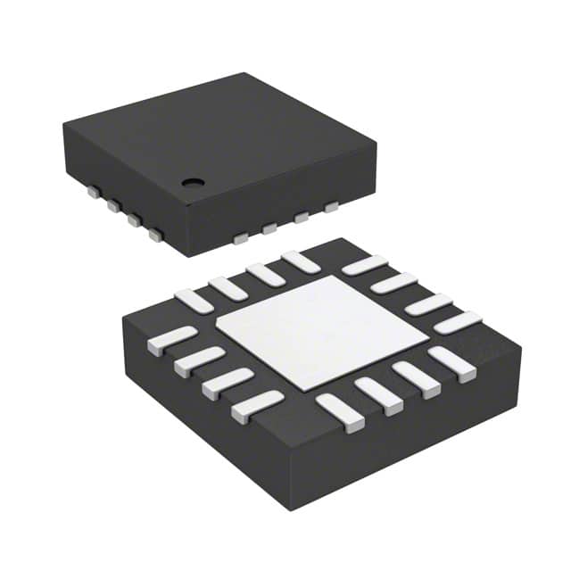
- Part No.:
- AP3615FNTR-G1
- Manufacturer:
- Diodes Incorporated
- Category:
- LED Drivers
- Package:
- 16-VFQFN Exposed Pad
- Datasheet:
-
 AP3615FNTR-G1.pdf
- Description:
- IC LED DRV RGLTR MULT-STEP 16QFN
- Quantity:
- Payment:

- Shipping:

Inventory:4,762
Please send an inquiry. Send us your inquiry, and we will respond immediately.
Product details
Overview
AP3615FNTR-G1 from Diodes Incorporated is a 5-channel charge pump LED driver IC with integrated low-dropout current sinks, designed for white LED backlighting in portable displays. It delivers up to 20 mA per channel across five independent WLEDs, supports 1x/1.5x auto-select charge pump operation, operates from 2.8 V to 5.5 V (Li-ion compatible), and features 16-step digital pulse dimming via the EN pin.
For engineers reviewing the AP3615FNTR-G1 datasheet, AP3615FNTR-G1 pinout, AP3615FNTR-G1 application, or AP3615FNTR-G1 equivalent, this page provides verified functional identity, validated QFN-3×3-16 pin mapping, confirmed current matching (±3%), thermal shutdown (160°C), and real-world dimming timing constraints (tLO: 0.1–500 µs, tHI > 0.1 µs).
Technical Context
The AP3615FNTR-G1 integrates a 1 MHz fixed-frequency charge pump with automatic 1x/1.5x mode selection based on input voltage and load conditions-transitioning at VIN ≈ 3.5 V (falling) and 3.7 V (rising). Its five matched current sinks each regulate output with ±3% matching over temperature and supply variation.
Digital brightness control is implemented exclusively through pulse-width modulation on the EN pin, enabling 16 discrete current levels without external DAC or I²C interface. Internal soft-start limits inrush current to 320 mA, and protection includes UVLO (2.2 V threshold), OVP (5.5 V), and OTSD (160°C with 20°C hysteresis).
Key Specifications
| Parameter | Value and Actual Design Meaning |
|---|---|
| Output Current per Channel | 20 mA typical, 18.5–21.5 mA over full operating range-enables consistent brightness across 5 WLEDs in series-parallel backlight arrays. |
| Current Matching | ±3% between any two outputs at VF = 3.2 V-minimizes visible luminance variation in multi-LED display zones. |
| Charge Pump Frequency | 1 MHz typical (0.7–1.3 MHz)-allows use of compact 1 µF ceramic flying/output capacitors, reducing board area and BOM cost. |
| Input Voltage Range | 2.8 V to 5.5 V-fully supports single-cell Li-ion battery operation including discharge down to 2.8 V without dropout. |
| Dimming Control | 16-step digital pulse dimming via EN pin (tLO = 0.1–500 µs, tHI > 0.1 µs)-eliminates need for external PWM generator or I²C controller. |
| Thermal Shutdown | Activates at TJ = +160°C with +20°C hysteresis-prevents permanent damage during sustained high-current or high-ambient operation. |
| UVLO Threshold | 2.2 V falling threshold with 250 mV hysteresis-ensures clean startup and prevents brown-out oscillation near battery EOL. |
Pinout & Package
AP3615FNTR-G1 is housed in a thermally enhanced QFN-3×3-16 package with exposed pad connected to AGND. The 3 mm × 3 mm footprint supports high-density portable PCB layouts and efficient heat dissipation via the bottom thermal pad.
| Pin/Terminal | Circuit Role | Design Meaning |
|---|---|---|
| 1 C1− | Flying capacitor 1 negative terminal | Must be routed with minimal trace length to C1− pad of 1 µF flying cap; critical for charge pump stability and EMI control. |
| 2 C2− | Flying capacitor 2 negative terminal | Low-inductance connection required to C2− of second 1 µF flying capacitor; separates charge paths for 1x/1.5x mode integrity. |
| 3 C2+ | Flying capacitor 2 positive terminal | Connects to C2+ of second flying cap; enables dual-capacitor charge transfer architecture for higher efficiency in 1.5x mode. |
| 4 C1+ | Flying capacitor 1 positive terminal | Primary charge transfer node for 1x mode; routing proximity to C1+ minimizes switching loop area and radiated noise. |
| 5 AGND | Analog ground reference | Reference for internal bandgap, current sense, and dimming logic; must be separated from PGND and tied to exposed pad. |
| 6 PGND | Power ground return | High-current return path for charge pump switching and LED sink currents; requires low-impedance copper pour under IC. |
| 7 VIN | Main power input | Accepts 2.8–5.5 V; bypassed with 1 µF ceramic capacitor placed adjacent to pin to suppress input ripple and supply transients. |
| 8 EN | Enable/dimming control input | Logic-high enables operation; pulse-width modulated signal here sets 16 brightness levels-no pull-up required. |
| 9–13 D1–D5 | WLED cathode current sinks | Each sinks up to 20 mA; unused pins must be tied to VIN to disable channel and prevent floating node instability. |
| 14 VOUT2 | Charge pump output distribution rail | Powers all five current sinks; connects externally to VOUT1 via PCB trace as specified (Pin 14 → Pin 16). |
| 15 NC | No connection | Internally unconnected; must remain unpopulated and unconnected on PCB to avoid parasitic coupling. |
| 16 VOUT1 | Primary charge pump output | Main boosted output node; requires 1 µF ceramic capacitor placed within 2 mm for ripple suppression and loop stability. |
Key Features
| Feature | Design Value |
|---|---|
| Regulated current matching | ±3% matching between any two channels ensures uniform luminance across multi-zone LCD backlights without per-channel calibration. |
| Auto-switching charge pump modes | Seamlessly transitions between 1x (bypass) and 1.5x (step-up) based on VIN and load-maximizes efficiency across full battery discharge curve. |
| Integrated soft-start | 200 µs controlled ramp limits peak inrush current to 320 mA-prevents voltage droop on shared battery rails during power-up. |
| Single-pin digital dimming | EN pin accepts standard logic-level pulses (0.1–500 µs low time); eliminates need for dedicated PWM controller or serial interface. |
| Comprehensive protection suite | Includes UVLO, OVP (5.5 V), OTSD (160°C), and open-LED detection-reduces system-level fault monitoring overhead. |
Applications
| Smartphone Backlight | PDA Display Driver |
|---|---|
|
Use Scenario: Driving 5 parallel white LEDs behind an HD LCD panel in a battery-powered smartphone. IC Role / Device Role / Timing Role: Charge pump LED driver with integrated current sinks and EN-based dimming control. Use Value: Maintains consistent brightness across 5 LEDs at 20 mA each while operating down to 2.8 V battery voltage-extending usable screen-on time. |
Use Scenario: Powering segmented WLED backlight in handheld PDA with variable ambient light conditions. IC Role / Device Role / Timing Role: Efficient current-regulated LED driver supporting 16-step manual or software-controlled brightness adjustment. Use Value: Eliminates external PWM generator and reduces component count by using EN pin for direct microcontroller dimming control. |
| Portable Media Player | Industrial HMI Display |
|
Use Scenario: Backlighting a 3.5-inch TFT display in an MP4 player powered by single-cell Li-ion. IC Role / Device Role / Timing Role: Step-up DC-DC converter with low-dropout current regulation and thermal protection. Use Value: Delivers stable 20 mA per LED across −40°C to +85°C ambient-ensuring reliable operation in automotive or outdoor environments. |
Use Scenario: Driving ruggedized display backlight in factory-floor HMIs where long-term reliability and thermal robustness are critical. IC Role / Device Role / Timing Role: Protected LED driver with UVLO, OVP, and OTSD-reducing field failure risk from power anomalies or overheating. Use Value: Built-in 160°C thermal shutdown with 20°C hysteresis prevents latch-up and enables safe recovery after transient overload events. |
Availability
AP3615FNTR-G1 is available at Aetrix Electronics and suitable for smartphone backlighting, portable media player displays, industrial HMI panels, and PDA applications requiring stable component supply and legacy design continuity.
Supply support for AP3615FNTR-G1 includes scheduled delivery planning, volume procurement assistance, BOM continuity management, traceable sourcing, and lifecycle availability coordination for OEM customers, industrial embedded developers, connected-device designers, and electronics production programs.
Manufacturer
Diodes Incorporated is a global manufacturer of discrete semiconductors and analog ICs, specializing in high-efficiency power management, signal integrity, and lighting solutions for consumer, industrial, and computing markets.
The AP3615 belongs to Diodes' LED backlight driver product line, engineered specifically for space-constrained portable devices requiring high-current matching, wide input voltage tolerance, and minimal external components.
FAQ
What is the recommended external capacitor configuration for AP3615FNTR-G1?
The AP3615FNTR-G1 requires four 1 µF X5R/X7R ceramic capacitors: one 1 µF input capacitor (CIN) at VIN, two 1 µF flying capacitors (C1, C2) connected to pins C1± and C2±, and one 1 µF output capacitor (COUT) at VOUT1. All must be placed within 2 mm of their respective pins with short, wide traces to minimize ESR and ESL.
How does the EN pin implement 16-step dimming without an I²C interface?
The EN pin uses pulse-counting dimming: each low-pulse with duration 0.1–500 µs increments a 4-bit counter, reducing LED current by 1/16 per pulse. After 15 pulses, current drops to 1/16 of full scale; a final pulse resets to 100%. No clock or data lines are needed-only a GPIO capable of generating precise µs-width pulses.
Can unused LED sink pins (e.g., D3–D5) be left floating?
No. Unused sink pins (D1–D5) must be connected directly to VIN to disable the channel. Floating these pins risks unpredictable current leakage, instability in the charge pump regulation loop, or false triggering of open-LED protection. This requirement is explicitly stated in the datasheet pin description table.
Is AP3615FNTR-G1 still in active production despite "OBSOLETE" status noted in documentation?
Yes-while Diodes' datasheet revision notes state "PART OBSOLETE", Aetrix Electronics confirms active inventory and ongoing supply chain support for AP3615FNTR-G1 under its legacy component continuity program. No functional replacement has been designated by Diodes, and the part remains orderable through authorized distribution channels with full traceability.
AP3615FNTR-G1 Specifications
- Product attributes
- Attribute value
- Manufacturer:
- Diodes Incorporated
- Series:
- -
- Package/Case:
- 16-VFQFN Exposed Pad
- Packaging:
- Tape & Reel (TR)
- Product Status:
- Active
- Type:
- DC DC Regulator
- Topology:
- Switched Capacitor (Charge Pump)
- Internal Switch(s):
- Yes
- Number of Outputs:
- 5
- Voltage - Supply (Min):
- 2.8V
- Voltage - Supply (Max):
- 5.5V
- Voltage - Output:
- -
- Current - Output / Channel:
- 20mA
- Frequency:
- 1MHz
- Dimming:
- Multi-Step
- Applications:
- Backlight
- Operating Temperature:
- -40°C ~ 85°C (TA)
- Grade:
- -
- Qualification:
- -
- Mounting Type:
- Surface Mount
- Supplier Device Package:
- 16-QFN (3x3)
AP3615FNTR-G1 FAQ
1.How can I place an order for AP3615FNTR-G1 through Aetrix?
Please submit a Request for Quotation (RFQ) for AP3615FNTR-G1 on Aetrix. Our sales agent will provide a competitive quotation and guide you through the order confirmation once you accept the terms.
2.Are the price and stock information for AP3615FNTR-G1 reliable?
The price and inventory of AP3615FNTR-G1 are updated periodically and may fluctuate due to market conditions. Stock and pricing data are typically refreshed every 24 hours. Quotation validity for AP3615FNTR-G1 is usually 5 days.
3.What payment methods are accepted for AP3615FNTR-G1?
We accept Wire Transfer, PayPal, Credit Card, Western Union, MoneyGram, and Escrow for AP3615FNTR-G1 transactions.
Note: Certain payment methods may incur a processing fee.
4.How is shipping managed for AP3615FNTR-G1?
AP3615FNTR-G1 orders can be shipped via leading logistics carriers, including DHL, UPS, FedEx, TNT, or Registered Mail.
Once your AP3615FNTR-G1 order is processed, you will receive an email with the shipment details and tracking number.
Note: Tracking information may take up to 24 hours to appear. Express delivery typically takes 3–5 business days.
5.How can I obtain technical support or documentation for AP3615FNTR-G1?
For technical support, including AP3615FNTR-G1 datasheets, pinout diagrams, or application guidance, please contact our engineering support team. They can provide detailed documentation and assistance for your AP3615FNTR-G1 requirements.
6.How does Aetrix verify that AP3615FNTR-G1 is sourced from the original manufacturer or authorized distributors?
All AP3615FNTR-G1 products on Aetrix are procured from qualified distributors and authorized channels. Our dedicated quality assurance team conducts strict verification, including traceability checks and, if necessary, third-party testing. This ensures that AP3615FNTR-G1 meets industry standards.
7.What is the process for return or replacement of AP3615FNTR-G1?
All AP3615FNTR-G1 units undergo pre-shipment inspection (PSI). If there is an issue with AP3615FNTR-G1, returns or replacements are accepted under the following conditions:
1.Quantity discrepancies, incorrect items, or visible external defects (such as breakage or corrosion), acknowledged by Aetrix.
2.The issue is reported within 90 days of delivery.
3.The AP3615FNTR-G1 part is unused and in its original packaging.
Return procedure for AP3615FNTR-G1:
1.Submit a request within 90 days.
2.Obtain a Return Material Authorization (RMA) from Aetrix.
AP3615FNTR-G1 Tags

-
BCR402RE6327HTSA1
Infineon Technologies

-
BCR430UXTSA2
Infineon Technologies

-
BCR420UE6433HTMA1
Infineon Technologies
-
BCR420UE6327HTSA1
Infineon Technologies
-
BCR421UE6327HTSA1
Infineon Technologies

-
LYT1604D-TL
Power Integrations

-
HV9910CLG-G
Microchip Technology

-
CL2N8-G
Microchip Technology

-
BCR420UW6-7
Diodes Incorporated
-
BCR421UW6-7
Diodes Incorporated

-
BCR420UFD-7
Diodes Incorporated
-
BCR421UFD-7
Diodes Incorporated
Tech Hub

An engineering guide to LED driver operation, constant-current and constant-voltage outputs, linear and switching topologies, dimming, IC selection, calculations, replacement compatibility, and fault c…

Operational amplifier guide covering op amp basics, feedback, ideal vs real op amps, common configurations, buffer circuits, offset, bias current, gain-bandwidth, slew rate, rail-to-rail limits and sel…

Jumper cables guide covering safe connection order, red and black clamp placement, final ground connection, cable gauge, length, clamp quality, copper vs CCA cables, jump starter comparison and battery…

LDO regulator guide covering low dropout voltage, power dissipation, thermal design, PSRR, output noise, capacitor stability, adjustable LDO circuits, LDO vs buck converter and datasheet selection chec…

Conditional Access Module guide covering CAM meaning, CI/CI+ interface, smart card authorization, DVB security workflow, TV and set-top box compatibility, internal electronics, ESD protection, connecto…

Guide to electronic component obsolescence covering EOL risk, PCN/PDN notices, last-time buy planning, replacement options, form-fit-function validation, counterfeit risk and BOM lifecycle management.

18650 battery guide covering lithium-ion cell basics, 3.6V/3.7V voltage, 4.2V charging, mAh and Wh capacity, protected cells, chargers, BMS, series-parallel packs, holders, welding and sourcing checks.…

Hall effect sensor guide covering working principle, linear and digital sensors, Arduino circuits, current sensing, speed detection, automotive applications, A3144 examples, signal filtering and datash…

Product Change Notification guide for electronic components, covering PCN meaning, PCN vs PDN/EOL, common change types, risk levels, form-fit-function review, engineering validation, BOM control, LTB/L…

A practical guide to blend door actuators, covering HVAC function, symptoms, location, AC and heater issues, reset and calibration, replacement cost, electrical diagnosis, compatibility checks, and rep…


