
 My Inquiry
 My Account


Diodes Incorporated AP43771VFBZ-13
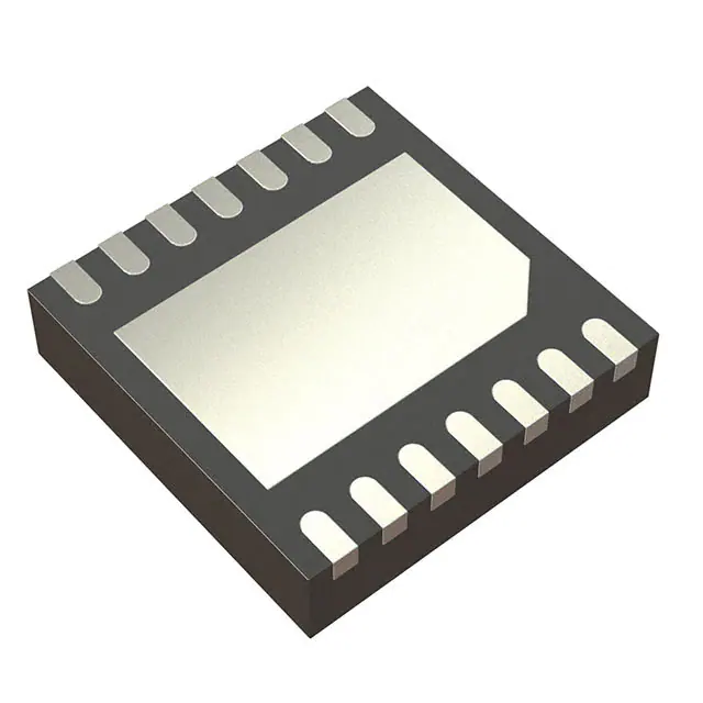
- Part No.:
- AP43771VFBZ-13
- Manufacturer:
- Diodes Incorporated
- Category:
- Controllers
- Package:
- 14-WFDFN Exposed Pad
- Datasheet:
-
 AP43771VFBZ-13.pdf
- Description:
- ACDC DECODER,W-DFN3030-14,T&R,3K
- Quantity:
- Payment:

- Shipping:

Inventory:2,949
Please send an inquiry. Send us your inquiry, and we will respond immediately.
Product details
Overview
AP43771VFBZ-13 from Diodes Incorporated is a USB Type-C® Power Delivery 3.1 controller with integrated 8-bit 1T 8051 MCU, supporting PPS (20 mV/step, 50 mA/step), QC4/4+/QC5, and USB-IF TID 4305 certification. It delivers up to 21 V programmable output in single-port 65 W USB PD chargers using standard firmware and resistor-selectable 8-power-profile menu via OTP pin. Its dual-loop CV/CC control drives optocoupled feedback for isolated flyback/buck-boost topologies.
For engineers reviewing the AP43771VFBZ-13 datasheet, AP43771VFBZ-13 pinout, AP43771VFBZ-13 application, or AP43771VFBZ-13 equivalent, key selection criteria include PPS resolution, CC/CV loop architecture, OTP-based profile selection, e-Marker cable detection, and built-in OVP/OCP/SCP/OTP protection with auto-restart - all validated for USB PD Rev3.1 V1.2 compliance.
Technical Context
The AP43771VFBZ-13 implements a dual-loop analog control architecture: CV regulation uses VFB input referenced to internal DACs (4.85–5.15 V for 5 V, 8.73–9.27 V for 9 V, 11.64–12.36 V for 12 V), while CC regulation uses IFB input with 10 mΩ current-sense resistor interface. Both loops drive OCDRV - an open-drain output for optocoupler base drive - enabling isolated primary-side feedback without secondary-side controllers.
It embeds a BMC physical layer for USB PD communication over CC1/CC2, supports SOP command execution for e-Marker detection, and integrates cable-loss compensation (22–42 mV/A adjustable). The device operates from 3.3 V to 24 V supply and includes dedicated hardware acceleration for QC2–QC5 and BC1.2 protocols, with DP/DN pins used for HVDCP negotiation.
Key Specifications
| Parameter | Value and Actual Design Meaning |
|---|---|
| USB PD Compliance | Rev3.1 V1.2 certified (TID 4305); supports full PPS up to 21 V with 20 mV/step voltage & 50 mA/step current resolution. |
| Protocol Support | Qualcomm QC2/3/4/4+/5, USB BC1.2, AFC, FCP, SCP - all implemented in dedicated hardware, not software emulation. |
| CV/CC Control | VFB reference: 4.85–5.15 V (5 V), 8.73–9.27 V (9 V), 11.64–12.36 V (12 V); IFB reference set by DAC; OCDRV open-drain output drives optocoupler LED directly. |
| Protection Features | Built-in OVP (5.6–6.8 V @5 V, 9.9–12.1 V @9 V), UVP (3.3–4.4 V @5 V), SCP, OTP (140 °C trip), auto-restart on fault clearance. |
| Power Supply Range | VCC = 3.3 V to 24 V; internal 5 V LDO (V5V) and 3 V LDO (V3VD in QFN24 variant); deep-sleep ICC = 550–900 μA after CC detach. |
| Package & Pin Count | W-DFN3030-14 (Type A1), 14-pin, 3.0 mm × 3.0 mm × 0.75 mm; θJA = 54 °C/W; RoHS, halogen-free, lead-free. |
| Current Sensing | ISENP input accepts 10 mΩ sense resistor; supports high-efficiency CC regulation with minimal power loss and thermal impact. |
Pinout & Package
AP43771VFBZ-13 is housed in a thermally enhanced W-DFN3030-14 (Type A1) package - 3.0 mm × 3.0 mm, 0.75 mm height, exposed thermal pad, RoHS-compliant matte tin finish.
| Pin | Circuit Role | Design Meaning |
|---|---|---|
| VBUS | Discharge path terminal | Sinks ~200 mA internally during PDO transition/cable detach to meet USB PD discharge timing requirements. |
| PWR_EN | nMOS gate driver output | Charge-pump boosted high-side gate drive for external nMOS switch; requires 10 Ω series resistor to gate. |
| VCC | Main IC power supply | 3.3–24 V input; requires 1 μF ceramic capacitor to GND; powers internal LDOs, MCU, and analog blocks. |
| ISENP | Current sense positive input | Connects to high-side of 10 mΩ shunt; enables precise CC regulation with low offset and noise sensitivity. |
| OCDRV | Open-drain CV/CC output | Drives optocoupler LED directly; dual-loop output shared between CV and CC paths for isolated feedback control. |
| GND | Analog/digital ground reference | Single ground plane required; connects to PCB thermal pad for thermal dissipation and noise immunity. |
| OTP | Profile selection / NTC interface | 100 μA current source; resistor-to-ground selects one of 8 preloaded power profiles (e.g., 5 V/3 A, 9 V/3 A, 12 V/5 A). |
| VFB | CV feedback input | Negative input of CV opamp; senses scaled VBUS via resistor divider; sets target voltage via internal DAC reference. |
| IFB | CC feedback input | Negative input of CC opamp; compares I×Rsense drop against DAC-set threshold for constant-current regulation. |
| CC2 / CC1 | Type-C configuration channel | Dual CC pins detect cable attach/detach, orientation, Rp/Rd values, and e-Marker presence via BMC signaling. |
| DN / DP | USB 2.0 data lines | Support HVDCP protocol negotiation (QC/AFC/FCP/SCP) via D+/- line voltage detection and signaling. |
| V5V | Internal 5 V LDO output | Supplies 5 V at up to 50 mA; requires 1 μF ceramic cap to GND; powers external logic or level-shifters. |
Key Features
| Feature | Design Value |
|---|---|
| Resistor-selectable power profiles | 8 preloaded USB PD profiles (e.g., 5 V/3 A, 9 V/3 A, 12 V/5 A, 15 V/3 A, 20 V/3.25 A) selected via single OTP-pin resistor - eliminates OTP programming cost and simplifies BOM. |
| Integrated BMC PHY & protocol engine | Fully hardware-accelerated USB PD Rev3.1 stack including packet encoding/decoding, CRC, SOP command execution, and e-Marker detection - no host MCU dependency. |
| Dual-loop analog CV/CC control | Independent VFB and IFB inputs with DAC-referenced opamps drive shared OCDRV output - enables stable, monotonic voltage transitions without digital loop latency. |
| Cable-loss compensation | Adjustable 0–7×VCABLE (22–42 mV/A) compensation applied to CV loop - maintains accurate output voltage at load under varying cable resistance. |
| Robust protection suite | Hardware-based OVP/UVP/SCP/OTP with fixed thresholds and deglitch timers (e.g., 30 ms OCP deglitch, 0.8 s SCP restart interval) - ensures fail-safe operation without firmware intervention. |
Applications
| Single-Port USB PD Charger | Dual-Port Smart Power Sharing |
|---|---|
|
Use Scenario: 65 W wall adapter for laptops and tablets with single Type-C port. IC Role / Device Role / Timing Role: Primary-side USB PD protocol controller and CV/CC regulator; manages PDO negotiation, VBUS enable/disable, and optocoupler feedback timing. Use Value: Enables resistor-based profile selection (no firmware update needed), meets USB PD Rev3.1 discharge timing (<2 s), and supports PPS for fast-charging smartphones. |
Use Scenario: 100 W dual-C-port travel charger allocating power dynamically between laptop and phone. IC Role / Device Role / Timing Role: Master/slave USB PD controller with I2C coordination; monitors port status and reallocates power profiles in <100 ms via embedded MCU. Use Value: Achieves intelligent power sharing without external microcontroller; leverages GPIO and I2C (in QFN24 variant) to coordinate multi-port negotiation and prevent overloading. |
| QC-Compatible Wall Adapter | USB PD + BC1.2 Automotive Charger |
|
Use Scenario: Compact 18 W QC4+ wall adapter for Android smartphones. IC Role / Device Role / Timing Role: HVDCP protocol handler using DP/DN pins; performs QC handshake within 500 ms and regulates VBUS via OCDRV-driven optocoupler. Use Value: Hardware-accelerated QC2–QC5 support ensures compatibility with legacy QC devices while maintaining USB PD readiness for future upgrades. |
Use Scenario: In-car USB PD charger with dual Type-C ports supporting both PD and legacy BC1.2 devices. IC Role / Device Role / Timing Role: Dual-role controller managing BC1.2 D+/- detection and PD CC negotiation simultaneously; handles cold-socket detection and VCONN switching. Use Value: Single-chip solution eliminates need for separate BC1.2 and PD controllers; supports simultaneous negotiation with mixed-device ecosystems (e.g., iPhone + Samsung Galaxy). |
Equivalent & Alternatives
The following parts are listed as comparable options for similar USB PD controller applications.
| Alternative Part | Technical Difference | Application Difference | Selection Advice |
|---|---|---|---|
| STUSB4500QTR | Standalone USB PD sink controller (no source capability); lacks QC protocol support and OTP-based profile selection. | Only suitable for sink-only applications (e.g., power banks); cannot replace AP43771VFBZ-13 in source-mode adapters. | Select only if designing a USB PD sink device requiring USB-IF certification without QC or PPS source functionality. |
| IP2721 | Integrated PD3.1 source controller with built-in MOSFET drivers; supports 32 V VBUS but no hardware QC acceleration - relies on firmware for QC4/5. | Higher integration (no external nMOS needed) but longer firmware validation cycle; lacks resistor-selectable profiles - requires OTP programming per SKU. | Prefer for space-constrained designs where gate-driver integration offsets added firmware complexity and qualification time. |
Compared with STUSB4500QTR and IP2721, AP43771VFBZ-13 uniquely combines hardware-accelerated QC protocols, resistor-selectable 8-profile menu, and dual-loop analog CV/CC control - enabling faster time-to-market for certified 65 W USB PD source adapters without firmware development or OTP programming overhead.
Availability
AP43771VFBZ-13 is available at Aetrix Electronics and suitable for USB PD 3.1 single-port chargers, QC4+/QC5 wall adapters, and automotive dual-C-port power supplies requiring stable component supply, long-lifecycle support, and full USB-IF TID 4305 compliance.
Supply support for AP43771VFBZ-13 includes scheduled delivery planning, volume procurement assistance, BOM continuity management, traceable sourcing, and lifecycle availability coordination for OEM customers, industrial embedded developers, connected-device designers, and electronics production programs.
Manufacturer
Diodes Incorporated is a global semiconductor manufacturer specializing in discrete, analog, and mixed-signal ICs, with design centers in Asia, Europe, and the US, and manufacturing in IATF 16949-certified facilities.
The AP43771V belongs to Diodes' USB Power Delivery Controller product line, engineered specifically for high-efficiency, certification-ready USB PD source implementations in compact AC-DC adapters and portable chargers - emphasizing hardware protocol acceleration, analog loop stability, and simplified system-level qualification.
FAQ
What is the function of the OTP pin on AP43771VFBZ-13?
The OTP pin provides a 100 µA current source used to select one of eight preloaded USB PD power profiles via an external resistor to ground. This eliminates the need for OTP programming during manufacturing and simplifies inventory management across multiple output configurations (e.g., 5 V/3 A, 9 V/3 A, 12 V/5 A). The resistor value determines the profile index based on factory-trimmed thresholds.
Does AP43771VFBZ-13 support Programmable Power Supply (PPS)?
Yes, AP43771VFBZ-13 fully supports USB PD Rev3.1 PPS with 20 mV/step voltage resolution and 50 mA/step current resolution. It implements PPS APDO (Augmented Power Data Object) negotiation in hardware, enabling dynamic voltage/current adjustment during charging - critical for fast-charging smartphones like Samsung Galaxy and Google Pixel devices.
How does the AP43771VFBZ-13 handle overvoltage protection?
AP43771VFBZ-13 provides hardware-based OVP with fixed thresholds: 5.6–6.8 V for 5 V mode, 9.9–12.1 V for 9 V mode, and 13.2–16.2 V for 12 V mode. Upon detection, it disables the PWR_EN signal within 50 µs and activates internal VBUS discharge (~200 mA sink) to meet USB PD specification timing. Recovery requires fault clearance and automatic restart after 0.8 s for SCP events.
Can AP43771VFBZ-13 be used in dual-port USB PD designs?
Yes - when paired with the W-QFN4040-24 variant (AP43771VDKZ-13), which adds I2C, GPIOs, and V3VD LDO, the AP43771VFBZ-13's firmware architecture supports master/slave coordination. The master device monitors port status via I2C and reassigns power profiles to slave ports in real time, enabling intelligent power sharing without external microcontroller intervention.
AP43771VFBZ-13 Specifications
- Product attributes
- Attribute value
- Manufacturer:
- Diodes Incorporated
- Package/Case:
- 14-WFDFN Exposed Pad
- Programmable:
- Not Verified
- Protocol:
- I2C
- Function:
- Controller
- Interface:
- I2C, USB
- Standards:
- USB 3.0
- Voltage - Supply:
- 3.3V ~ 24V
- Current - Supply:
- 6mA
- Operating Temperature:
- -40°C ~ 85°C
- Supplier Device Package:
- W-DFN3030-14 (Type A1)
- Grade:
- -
- Qualification:
- -
AP43771VFBZ-13 FAQ
1.How can I place an order for AP43771VFBZ-13 through Aetrix?
Please submit a Request for Quotation (RFQ) for AP43771VFBZ-13 on Aetrix. Our sales agent will provide a competitive quotation and guide you through the order confirmation once you accept the terms.
2.Are the price and stock information for AP43771VFBZ-13 reliable?
The price and inventory of AP43771VFBZ-13 are updated periodically and may fluctuate due to market conditions. Stock and pricing data are typically refreshed every 24 hours. Quotation validity for AP43771VFBZ-13 is usually 5 days.
3.What payment methods are accepted for AP43771VFBZ-13?
We accept Wire Transfer, PayPal, Credit Card, Western Union, MoneyGram, and Escrow for AP43771VFBZ-13 transactions.
Note: Certain payment methods may incur a processing fee.
4.How is shipping managed for AP43771VFBZ-13?
AP43771VFBZ-13 orders can be shipped via leading logistics carriers, including DHL, UPS, FedEx, TNT, or Registered Mail.
Once your AP43771VFBZ-13 order is processed, you will receive an email with the shipment details and tracking number.
Note: Tracking information may take up to 24 hours to appear. Express delivery typically takes 3–5 business days.
5.How can I obtain technical support or documentation for AP43771VFBZ-13?
For technical support, including AP43771VFBZ-13 datasheets, pinout diagrams, or application guidance, please contact our engineering support team. They can provide detailed documentation and assistance for your AP43771VFBZ-13 requirements.
6.How does Aetrix verify that AP43771VFBZ-13 is sourced from the original manufacturer or authorized distributors?
All AP43771VFBZ-13 products on Aetrix are procured from qualified distributors and authorized channels. Our dedicated quality assurance team conducts strict verification, including traceability checks and, if necessary, third-party testing. This ensures that AP43771VFBZ-13 meets industry standards.
7.What is the process for return or replacement of AP43771VFBZ-13?
All AP43771VFBZ-13 units undergo pre-shipment inspection (PSI). If there is an issue with AP43771VFBZ-13, returns or replacements are accepted under the following conditions:
1.Quantity discrepancies, incorrect items, or visible external defects (such as breakage or corrosion), acknowledged by Aetrix.
2.The issue is reported within 90 days of delivery.
3.The AP43771VFBZ-13 part is unused and in its original packaging.
Return procedure for AP43771VFBZ-13:
1.Submit a request within 90 days.
2.Obtain a Return Material Authorization (RMA) from Aetrix.
AP43771VFBZ-13 Tags

-
PTN5150AHXMP
NXP USA Inc.

-
USB3740B-AI9-TR
Microchip Technology

-
USB3740B-AI2-TR
Microchip Technology

-
USB3300-EZK-TR
Microchip Technology
-
USB3300-EZK
Microchip Technology

-
FUSB340TMX
onsemi

-
FUSB302BMPX
onsemi

-
DP83826IRHBR
Texas Instruments

-
MCP2518FDT-E/QBB
Microchip Technology
-
FUSB302MPX
onsemi

-
MCP2518FDT-E/SL
Microchip Technology

-
FT260Q-R
FTDI, Future Technology Devices International Ltd
Tech Hub

An engineering guide to LED driver operation, constant-current and constant-voltage outputs, linear and switching topologies, dimming, IC selection, calculations, replacement compatibility, and fault c…

Operational amplifier guide covering op amp basics, feedback, ideal vs real op amps, common configurations, buffer circuits, offset, bias current, gain-bandwidth, slew rate, rail-to-rail limits and sel…

Jumper cables guide covering safe connection order, red and black clamp placement, final ground connection, cable gauge, length, clamp quality, copper vs CCA cables, jump starter comparison and battery…

LDO regulator guide covering low dropout voltage, power dissipation, thermal design, PSRR, output noise, capacitor stability, adjustable LDO circuits, LDO vs buck converter and datasheet selection chec…

Conditional Access Module guide covering CAM meaning, CI/CI+ interface, smart card authorization, DVB security workflow, TV and set-top box compatibility, internal electronics, ESD protection, connecto…

Guide to electronic component obsolescence covering EOL risk, PCN/PDN notices, last-time buy planning, replacement options, form-fit-function validation, counterfeit risk and BOM lifecycle management.

18650 battery guide covering lithium-ion cell basics, 3.6V/3.7V voltage, 4.2V charging, mAh and Wh capacity, protected cells, chargers, BMS, series-parallel packs, holders, welding and sourcing checks.…

Hall effect sensor guide covering working principle, linear and digital sensors, Arduino circuits, current sensing, speed detection, automotive applications, A3144 examples, signal filtering and datash…

Product Change Notification guide for electronic components, covering PCN meaning, PCN vs PDN/EOL, common change types, risk levels, form-fit-function review, engineering validation, BOM control, LTB/L…

A practical guide to blend door actuators, covering HVAC function, symptoms, location, AC and heater issues, reset and calibration, replacement cost, electrical diagnosis, compatibility checks, and rep…


