
 My Inquiry
 My Account


Diodes Incorporated AP9211SA-DD-HAC-7
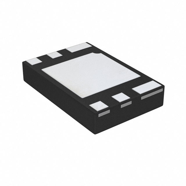
- Part No.:
- AP9211SA-DD-HAC-7
- Manufacturer:
- Diodes Incorporated
- Category:
- Battery Management
- Package:
- 6-UDFN Exposed Pad
- Datasheet:
-
 AP9211SA-DD-HAC-7.pdf
- Description:
- IC BATT PROT LI-ION 1CELL 6UDFN
- Quantity:
- Payment:

- Shipping:

Inventory:1,687
Please send an inquiry. Send us your inquiry, and we will respond immediately.
Product details
Overview
AP9211SA-DD-HAC-7 from Diodes Incorporated is a single-chip Li+ battery protection IC integrating dual n-channel MOSFETs (common-drain configuration), overcharge/overdischarge voltage detection (±25 mV accuracy at +25°C), discharge overcurrent sensing (0.05–0.32 V range, ±15 mV accuracy), and short-circuit protection (0.45–0.7 V, ±100 mV). It operates in 1-cell Li-ion packs for portable power tools and medical handheld devices.
For engineers reviewing the AP9211SA-DD-HAC-7 datasheet, AP9211SA-DD-HAC-7 pinout, AP9211SA-DD-HAC-7 application, or AP9211SA-DD-HAC-7 equivalent, key selection criteria include its U-DFN2030-6 (Type C) package, 0.1 µA max power-down current, selectable 0V charge function, and integrated MOSFET RSS(ON) of 27 mΩ (typ) at VDD = 4.0 V.
Technical Context
The AP9211SA-DD-HAC-7 implements independent voltage monitoring paths for VDD–VSS (cell voltage) and VM–VSS (current-sense differential), with fixed delay timers (±20% accuracy at +25°C) for all protection events. Its logic circuitry controls gate drive to two internal MOSFETs using level-shifted signals to maintain operation across the full 1.5–5.5 V supply range.
It supports both power-down mode (0.1 µA max ICC) and auto-wake-up functionality: in overdischarge, the latter enables recovery without charger connection when battery voltage rises above VDU for tDLR, while the former requires external charging to exit sleep state. The VM pin interfaces with an external sense resistor (R2 = 2.7 kΩ typical) to detect charge/discharge current polarity and magnitude.
Key Specifications
| Parameter | Value and Actual Design Meaning |
|---|---|
| VCU Detection | 4.375 V ±25 mV - sets precise upper cell voltage limit before disabling charge path |
| VDL Detection | 2.500 V ±35 mV - prevents deep discharge damage by cutting off load at defined low-voltage threshold |
| VDOC Threshold | 0.150 V ±15 mV - corresponds to ~5.6 A discharge current with 27 mΩ RSS(ON), enabling accurate overcurrent trip |
| IQ Normal Mode | 3.0 µA typ - ultra-low quiescent current preserves battery standby life in always-connected applications |
| RSS(ON) | 27 mΩ typ @ VDD = 4.0 V - low on-resistance minimizes conduction loss and thermal rise during high-current discharge |
| tSHORT | 1.2 µs typ - fast short-circuit response protects battery and PCB traces from catastrophic fault energy |
| Package | U-DFN2030-6 (Type C), 2.0 × 3.0 × 0.55 mm - compact footprint with exposed thermal pad for efficient heat dissipation |
Pinout & Package
AP9211SA-DD-HAC-7 uses the U-DFN2030-6 (Type C) package with 6 terminals and an exposed thermal pad (EP). The EP serves as the common drain node for both internal MOSFETs and must be connected to a large copper pour for thermal management.
| Pin/Terminal | Circuit Role | Design Meaning |
|---|---|---|
| 1 S1 | Source of discharging MOSFET | Connects directly to battery negative terminal; carries full load current during discharge |
| 2 VSS | Negative power supply reference | Ground return for internal logic and voltage comparators; must be low-impedance |
| 3 VDD | Positive supply input | Connected to battery positive via R1 (330–470 Ω); powers internal circuitry and gate drivers |
| 4 NC | No connect | Internally unconnected; must remain floating per datasheet |
| 5 VM | Current-sense input | Monitors voltage drop across external R2 to detect charge/discharge direction and magnitude |
| 6 S2 | Source of charging MOSFET | Connects to charger negative input; carries full charge current when enabled |
| EP | Common drain / thermal pad | Shared drain node for both MOSFETs; requires PCB copper area for thermal conduction and electrical grounding |
Key Features
| Feature | Design Value |
|---|---|
| Integrated dual n-MOSFETs | Eliminates need for external discrete FETs and gate drivers, reducing BOM count and layout area |
| Programmable 0V battery charge | Factory-configured permission enables safe recharge of fully depleted cells without manual intervention |
| Overvoltage charger detection | 8.0 V fixed threshold (±2 V) disables charging if input exceeds safe level, protecting against faulty chargers |
| Auto-wake-up capability | Enables autonomous recovery from overdischarge when battery voltage recovers, eliminating mandatory charger presence |
| Fixed delay timers | Built-in timing circuits remove external RC components, improving consistency and board-level reliability |
Applications
| Power Tools | Medical Handheld Devices |
|---|---|
Use Scenario: Cordless drill/driver with 1-cell Li-ion pack subject to high pulse loads and accidental short circuits. IC Role / Device Role / Timing Role: Battery protection IC providing overcurrent cutoff (tSHORT = 1.2 µs), overdischarge lockout (VDL = 2.500 V), and MOSFET control. Use Value: Prevents thermal runaway during stall conditions and extends pack cycle life by enforcing strict voltage boundaries. | Use Scenario: Portable ultrasound or glucose monitor requiring reliable, long-term standby with zero-volt recovery capability. IC Role / Device Role / Timing Role: Single-chip protector managing charge enable/disable, 0V recharge permission, and ultra-low IQ (3.0 µA). Use Value: Enables field-deployed devices to recover autonomously after deep self-discharge without technician service. |
| Wearable Fitness Trackers | Bluetooth Headsets |
Use Scenario: Compact wearable with space-constrained 1-cell Li-ion battery and aggressive power management. IC Role / Device Role / Timing Role: Integrated protection solution delivering voltage monitoring, current sensing, and MOSFET switching in 2.0 × 3.0 mm footprint. Use Value: Reduces PCB area by replacing discrete protection IC + dual MOSFETs, while maintaining ±25 mV voltage accuracy. | Use Scenario: True wireless stereo headset needing robust short-circuit immunity during earbud insertion/removal. IC Role / Device Role / Timing Role: Fast-acting protector with 0.7 V short-detection threshold and sub-microsecond response (tSHORT = 1.2 µs). Use Value: Prevents audible pop/noise and battery damage caused by transient contact faults during mechanical mating. |
Equivalent & Alternatives
The following parts are listed as comparable options for similar battery protection applications.
| Alternative Part | Technical Difference | Application Difference | Selection Advice |
|---|---|---|---|
| Seiko Instruments S-8261AAB-M6T1U | Separate protection IC + external MOSFETs; no integrated FETs; 2.0 µA IQ; 3.0 V to 4.25 V VCU range | Requires additional FETs and gate resistors; larger total footprint; lower integration | Select when discrete FET selection (e.g., specific RDS(on), voltage rating) is required beyond AP9211's fixed 24 V/9 A capability |
| Ricoh RP506Kxx1x-TR-F | Integrated dual n-MOSFET; 2.5 µA IQ; fixed VCU = 4.25 V; no 0V charge option; no overvoltage charger detection | Lacks overvoltage charger monitoring and factory-programmable 0V charge; simpler feature set | Select for cost-sensitive consumer electronics where charger overvoltage risk is mitigated externally and 0V recovery is unnecessary |
Compared with S-8261AAB-M6T1U and RP506Kxx1x-TR-F, the AP9211SA-DD-HAC-7 delivers higher integration (no external FETs), unique overvoltage charger detection (8.0 V), and configurable 0V charge-making it optimal for space-constrained, safety-critical 1-cell Li+ systems requiring autonomous recovery and charger fault immunity.
Availability
AP9211SA-DD-HAC-7 is available at Aetrix Electronics and suitable for portable power tools, medical handheld devices, wearable fitness trackers, and Bluetooth headsets requiring stable component supply, long-term lifecycle support, and RoHS-compliant packaging.
Supply support for AP9211SA-DD-HAC-7 includes scheduled delivery planning, volume procurement assistance, BOM continuity management, traceable sourcing, and lifecycle availability coordination for OEM customers, industrial embedded developers, connected-device designers, and electronics production programs.
Manufacturer
Diodes Incorporated is a global manufacturer of discrete semiconductors and analog ICs, specializing in high-reliability power management, signal integrity, and protection solutions for industrial, computing, and consumer markets.
The AP9211 belongs to Diodes' battery protection IC product line, engineered specifically for compact, high-accuracy 1-cell Li+ battery pack safety-emphasizing low quiescent current, integrated MOSFETs, and configurable fault responses.
FAQ
What is the function of the VM pin on the AP9211SA-DD-HAC-7?
The VM pin is the current-sense input that monitors the voltage difference between itself and VSS to detect charge/discharge current direction and magnitude. It connects to an external sense resistor (R2) and interfaces with internal comparators for discharge overcurrent, short-circuit, and charge overcurrent protection. Its internal pull-up (RVMD) and pull-down (RVMS) resistors activate selectively during different fault states to ensure correct MOSFET control.
Does the AP9211SA-DD-HAC-7 support overvoltage protection for the charger input?
Yes-the AP9211SA-DD-HAC-7 includes a dedicated overvoltage charger detection circuit that monitors the voltage between VDD and VM pins. When this voltage exceeds 8.0 V (±2 V), the charging MOSFET is immediately disabled; release occurs at 7.3 V (±2 V). No delay timer is applied to this function, enabling instantaneous response to unsafe charger conditions.
How does the auto-wake-up mode differ from power-down mode in the AP9211SA-DD-HAC-7?
In auto-wake-up mode (enabled by 'A' suffix), the device remains active during overdischarge and can autonomously resume normal operation when battery voltage rises above VDU for tDLR. In power-down mode (default), the IC enters ultra-low-current sleep (≤0.1 µA) and requires external charger connection to reset-no autonomous recovery is possible without charging current.
What is the maximum continuous current the internal MOSFETs can handle?
The internal dual n-channel MOSFETs support 9.0 A continuous drain current at +25°C (VGS = 4.5 V) and 7.1 A at +70°C, with a maximum drain-source voltage rating of 24 V. Thermal performance depends on PCB copper area under the EP pad; the datasheet specifies 1000 mW maximum power dissipation on a JEDEC High-K test board.
AP9211SA-DD-HAC-7 Specifications
- Product attributes
- Attribute value
- Manufacturer:
- Diodes Incorporated
- Series:
- -
- Package/Case:
- 6-UDFN Exposed Pad
- Packaging:
- Tape & Reel (TR)
- Product Status:
- Active
- Function:
- Battery Protection
- Battery Chemistry:
- Lithium Ion
- Number of Cells:
- 1
- Fault Protection:
- Over Current, Over Voltage
- Interface:
- -
- Operating Temperature:
- -40°C ~ 85°C (TA)
- Grade:
- -
- Qualification:
- -
- Mounting Type:
- Surface Mount
- Supplier Device Package:
- U-DFN2030-6 (Type C)
AP9211SA-DD-HAC-7 FAQ
1.How can I place an order for AP9211SA-DD-HAC-7 through Aetrix?
Please submit a Request for Quotation (RFQ) for AP9211SA-DD-HAC-7 on Aetrix. Our sales agent will provide a competitive quotation and guide you through the order confirmation once you accept the terms.
2.Are the price and stock information for AP9211SA-DD-HAC-7 reliable?
The price and inventory of AP9211SA-DD-HAC-7 are updated periodically and may fluctuate due to market conditions. Stock and pricing data are typically refreshed every 24 hours. Quotation validity for AP9211SA-DD-HAC-7 is usually 5 days.
3.What payment methods are accepted for AP9211SA-DD-HAC-7?
We accept Wire Transfer, PayPal, Credit Card, Western Union, MoneyGram, and Escrow for AP9211SA-DD-HAC-7 transactions.
Note: Certain payment methods may incur a processing fee.
4.How is shipping managed for AP9211SA-DD-HAC-7?
AP9211SA-DD-HAC-7 orders can be shipped via leading logistics carriers, including DHL, UPS, FedEx, TNT, or Registered Mail.
Once your AP9211SA-DD-HAC-7 order is processed, you will receive an email with the shipment details and tracking number.
Note: Tracking information may take up to 24 hours to appear. Express delivery typically takes 3–5 business days.
5.How can I obtain technical support or documentation for AP9211SA-DD-HAC-7?
For technical support, including AP9211SA-DD-HAC-7 datasheets, pinout diagrams, or application guidance, please contact our engineering support team. They can provide detailed documentation and assistance for your AP9211SA-DD-HAC-7 requirements.
6.How does Aetrix verify that AP9211SA-DD-HAC-7 is sourced from the original manufacturer or authorized distributors?
All AP9211SA-DD-HAC-7 products on Aetrix are procured from qualified distributors and authorized channels. Our dedicated quality assurance team conducts strict verification, including traceability checks and, if necessary, third-party testing. This ensures that AP9211SA-DD-HAC-7 meets industry standards.
7.What is the process for return or replacement of AP9211SA-DD-HAC-7?
All AP9211SA-DD-HAC-7 units undergo pre-shipment inspection (PSI). If there is an issue with AP9211SA-DD-HAC-7, returns or replacements are accepted under the following conditions:
1.Quantity discrepancies, incorrect items, or visible external defects (such as breakage or corrosion), acknowledged by Aetrix.
2.The issue is reported within 90 days of delivery.
3.The AP9211SA-DD-HAC-7 part is unused and in its original packaging.
Return procedure for AP9211SA-DD-HAC-7:
1.Submit a request within 90 days.
2.Obtain a Return Material Authorization (RMA) from Aetrix.
AP9211SA-DD-HAC-7 Tags

-
BQ29700DSER
Texas Instruments

-
S-8241ABKMC-GBKT2G
ABLIC Inc.
-
S-8241ABPMC-GBPT2G
ABLIC Inc.

-
BQ27427YZFR
Texas Instruments

-
BQ27426YZFR
Texas Instruments

-
STC3117IJT
STMicroelectronics

-
STC3115IJT
STMicroelectronics

-
BQ76925RGER
Texas Instruments
-
NPM1100-QDAA-R
Nordic Semiconductor ASA

-
BQ27441DRZR-G1A
Texas Instruments

-
STC3115AIQT
STMicroelectronics

-
S-8252AAL-M6T1U
ABLIC Inc.
Tech Hub

An engineering guide to LED driver operation, constant-current and constant-voltage outputs, linear and switching topologies, dimming, IC selection, calculations, replacement compatibility, and fault c…

Operational amplifier guide covering op amp basics, feedback, ideal vs real op amps, common configurations, buffer circuits, offset, bias current, gain-bandwidth, slew rate, rail-to-rail limits and sel…

Jumper cables guide covering safe connection order, red and black clamp placement, final ground connection, cable gauge, length, clamp quality, copper vs CCA cables, jump starter comparison and battery…

LDO regulator guide covering low dropout voltage, power dissipation, thermal design, PSRR, output noise, capacitor stability, adjustable LDO circuits, LDO vs buck converter and datasheet selection chec…

Conditional Access Module guide covering CAM meaning, CI/CI+ interface, smart card authorization, DVB security workflow, TV and set-top box compatibility, internal electronics, ESD protection, connecto…

Guide to electronic component obsolescence covering EOL risk, PCN/PDN notices, last-time buy planning, replacement options, form-fit-function validation, counterfeit risk and BOM lifecycle management.

18650 battery guide covering lithium-ion cell basics, 3.6V/3.7V voltage, 4.2V charging, mAh and Wh capacity, protected cells, chargers, BMS, series-parallel packs, holders, welding and sourcing checks.…

Hall effect sensor guide covering working principle, linear and digital sensors, Arduino circuits, current sensing, speed detection, automotive applications, A3144 examples, signal filtering and datash…

Product Change Notification guide for electronic components, covering PCN meaning, PCN vs PDN/EOL, common change types, risk levels, form-fit-function review, engineering validation, BOM control, LTB/L…

A practical guide to blend door actuators, covering HVAC function, symptoms, location, AC and heater issues, reset and calibration, replacement cost, electrical diagnosis, compatibility checks, and rep…


