
 My Inquiry
 My Account


Diodes Incorporated AP9214LA-AA-HSB-7
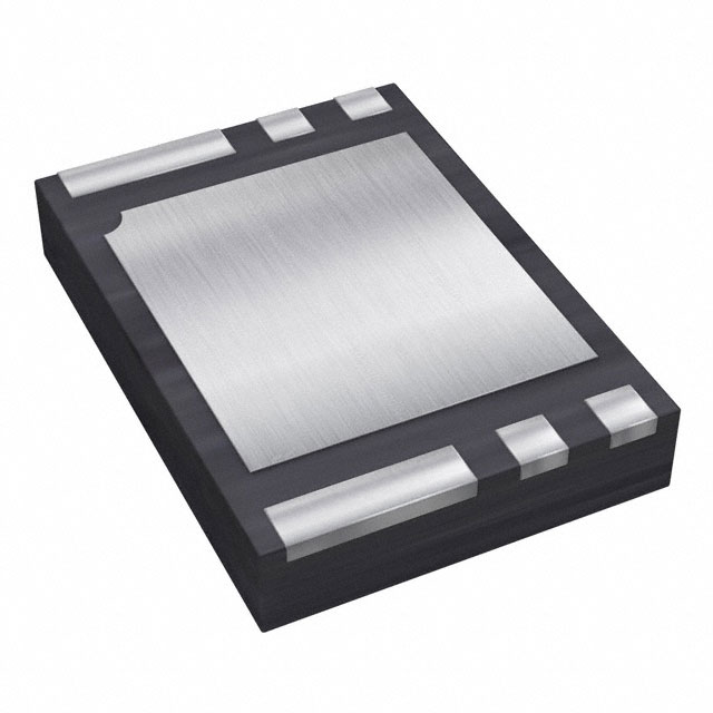
- Part No.:
- AP9214LA-AA-HSB-7
- Manufacturer:
- Diodes Incorporated
- Category:
- Battery Management
- Package:
- 6-UDFN Exposed Pad
- Datasheet:
-
 AP9214LA-AA-HSB-7.pdf
- Description:
- IC BATT PROT LI-ION 1CELL 6UDFN
- Quantity:
- Payment:

- Shipping:

Inventory:2,090
Please send an inquiry. Send us your inquiry, and we will respond immediately.
Product details
Overview
AP9214LA-AA-HSB-7 from Diodes Incorporated is a single-chip Li+ battery protection IC integrating dual N-channel MOSFETs (RSS(ON) ≤16 mΩ @ 4.0V), overcharge/overdischarge voltage detection (±25 mV accuracy), discharge overcurrent sensing (±15 mV), and short-circuit protection with 1 μs response. It operates in 1-cell Li+ packs for portable power tools, Bluetooth headsets, and medical wearables.
For engineers reviewing the AP9214LA-AA-HSB-7 datasheet, AP9214LA-AA-HSB-7 pinout, AP9214LA-AA-HSB-7 application, or AP9214LA-AA-HSB-7 equivalent, key selection criteria include integrated MOSFET RDS(on), 0.1 µA power-down current, selectable 0V charge function, and U-DFN2535-6 (Type B, Option 1) package compatibility with high-density PCB layouts.
Technical Context
The AP9214LA-AA-HSB-7 implements dual independent protection paths: one for charging (controlled via S2/VM/VDD) and one for discharging (via S1/VM/VSS), each with dedicated voltage and current thresholds. Its logic circuit uses internal level-shifted drivers to control two N-channel MOSFETs sharing a common drain (EP pad).
It features factory-programmed fixed delay timers (e.g., tCU = 1.0 s typ, ±20% accuracy) and supports either power-down mode (0.1 µA standby) or auto-wake-up operation. The VM pin senses bidirectional current through an external sense resistor (R2 = 2.7 kΩ typical), enabling precise overcurrent and short-circuit detection without external comparators.
Key Specifications
| Parameter | Value and Actual Design Meaning |
|---|---|
| VDD Operating Range | 1.5 V to 5.5 V - supports full Li+ cell voltage range (2.5–4.2 V) with margin for transient spikes. |
| Overcharge Detection Voltage | 4.250 V ±25 mV - factory-set for standard Li+ chemistry; prevents cell degradation above safe voltage. |
| Discharge Overcurrent Threshold | 0.100 V ±15 mV - sets 10 A cutoff with 10 mΩ sense resistor; enables accurate current limiting without calibration. |
| Quiescent Current (Normal) | 3.0 µA typ @ 25°C - extends battery shelf life in storage; low enough to avoid measurable self-discharge contribution. |
| Power-Down Current | 0.1 µA max - reduces standby drain to <1 µAh/month; critical for long-term unattended devices like IoT sensors. |
| MOSFET RSS(ON) | 13 mΩ max @ VDD = 4.0 V - limits conduction loss to <530 mW at 9 A continuous, reducing thermal stress in compact packs. |
| Short-Circuit Response Time | 1.0 µs typ - detects hard shorts before wire fusing or cell venting occurs; protects against catastrophic failure. |
Pinout & Package
Package: U-DFN2535-6 (Type B), 2.5 mm × 3.5 mm × 0.55 mm, exposed thermal pad (EP), RoHS-compliant, halogen-free.
| Pin/Terminal | Circuit Role | Design Meaning |
|---|---|---|
| S1 | Discharge MOSFET source | Connects directly to battery negative terminal; carries full load current during discharge. |
| VSS | Negative supply reference | Ground return for internal logic and voltage comparators; must be low-impedance path. |
| VDD | Positive supply input | Connected to battery positive via R1 (330–470 Ω); powers internal circuitry and gate drivers. |
| VM | Current sense and charger monitor | Measures voltage drop across R2 to detect charge/discharge current polarity and magnitude. |
| NC | No connect | Pin 5 in HSB option - must remain floating; no internal connection or pull-up/down. |
| EP | Common drain thermal pad | Shared drain node for both MOSFETs; requires large copper pour for heat dissipation and low-inductance switching. |
Key Features
| Feature | Design Value |
|---|---|
| Dual integrated N-MOSFETs | Eliminates need for external discrete FETs and gate drivers; reduces BOM count and layout area by >40%. |
| Factory-configured thresholds | VCU = 4.250 V, VDL = 2.500 V, VDOC = 0.100 V - eliminates external resistor networks and trimming for production consistency. |
| Selectable 0V battery charge | Enables recovery of deeply discharged cells (0 V) without manual pre-charge circuitry; improves field reliability. |
| Overvoltage charger detection | Triggers at 8.0 V ±2 V between VDD and VM - safeguards against faulty or mismatched chargers in multi-vendor ecosystems. |
| Two pin-out options | HSB (Option 1) places NC on Pin 5; HSBR (Option 2) places NC on Pin 4 - allows routing flexibility in constrained layouts. |
Applications
| Power Tool Battery Packs | Wireless Earbuds |
|---|---|
|
Use Scenario: Cordless drill battery pack with 1S Li+ cell, subjected to high-pulse discharge (≥15 A) and fast recharging. IC Role / Device Role / Timing Role: Primary protection controller monitoring cell voltage, discharge current, and short circuits in real time; disables discharge path within 1 µs during fault. Use Value: Prevents thermal runaway during motor stall events while maintaining <3 µA quiescent draw during idle, extending shelf life. |
Use Scenario: Compact true wireless stereo (TWS) earbud with space-constrained 1S 50 mAh Li+ cell and USB-C charging. IC Role / Device Role / Timing Role: Dual-path protector enabling simultaneous charge control (via S2/VM) and discharge control (via S1/VM) with shared sense resistor. Use Value: Integrates protection + dual MOSFETs in 2.5 × 3.5 mm footprint, freeing >1.2 mm² PCB area vs. discrete solutions. |
| Portable Medical Monitors | Smart Wearable Fitness Trackers |
|
Use Scenario: FDA-classified wearable ECG monitor requiring >2-year shelf life and guaranteed startup from 0 V after storage. IC Role / Device Role / Timing Role: Enables 0V battery charge function and ultra-low 0.1 µA power-down current to meet IEC 62304 standby requirements. Use Value: Eliminates need for external wake-up circuitry or backup coin cell; certified design reuse across Class II devices. |
Use Scenario: Slim wristband with 1S Li+ cell, frequent partial charge cycles, and aggressive power management. IC Role / Device Role / Timing Role: Auto-wake-up mode (AP9214LA) recovers from overdischarge without charger presence when battery voltage rises above VDU. Use Value: Supports user-initiated recovery after accidental deep discharge - avoids "bricked" device returns in consumer channels. |
Equivalent & Alternatives
The following parts are listed as comparable options for similar 1-cell Li+ battery protection applications.
| Alternative Part | Technical Difference | Application Difference | Selection Advice |
|---|---|---|---|
| Seiko Instruments S-8261AAB-M6T1U | Separate charge/discharge FETs; no integrated MOSFETs; higher quiescent current (1.5 µA min). | Requires external 2× N-MOSFETs and gate resistors; increases layout area and component count. | Preferred where discrete FET selection (e.g., 3.5 mΩ) is required for ultra-low-loss designs. |
| Ricoh RP507K001B-TR-F | Single integrated MOSFET only; no dual-path architecture; lacks 0V charge and overvoltage charger detection. | Supports charge-only or discharge-only protection; not suitable for bidirectional current monitoring. | Used in cost-sensitive single-function applications where charger overvoltage risk is mitigated externally. |
Compared with S-8261AAB-M6T1U and RP507K001B-TR-F, the AP9214LA-AA-HSB-7 delivers lower system-level BOM cost and smaller footprint via dual integrated MOSFETs, while adding unique functions like 8.0 V charger overvoltage detection and factory-set 0V charge enable - critical for medical and premium consumer designs.
Availability
AP9214LA-AA-HSB-7 is available at Aetrix Electronics and suitable for power tool battery packs, wireless earbuds, and portable medical monitors requiring stable component supply, long-term lifecycle support, and automotive-grade traceability.
Supply support for AP9214LA-AA-HSB-7 includes scheduled delivery planning, volume procurement assistance, BOM continuity management, traceable sourcing, and lifecycle availability coordination for OEM customers, industrial embedded developers, connected-device designers, and electronics production programs.
Manufacturer
Diodes Incorporated is a global semiconductor company specializing in discrete, analog, and mixed-signal ICs, with manufacturing certified to IATF 16949 and AEC-Q200 standards.
The AP9214L series belongs to Diodes' battery protection product line, engineered specifically for space-constrained, high-reliability 1-cell Li+ applications where integration, ultra-low quiescent current, and robust fault coverage are mandatory.
FAQ
What is the function of the NC pin on AP9214LA-AA-HSB-7?
The NC (No Connect) pin on AP9214LA-AA-HSB-7 is Pin 5 in the U-DFN2535-6 (Type B, Option 1) package. It has no internal connection and must remain electrically floating - no pull-up, pull-down, or PCB trace should attach to it. This pin exists solely for mechanical symmetry and package compatibility with Option 2 (HSBR), where NC is relocated to Pin 4.
Does AP9214LA-AA-HSB-7 support automatic recovery from overdischarge without a charger?
Yes - the "A" suffix denotes auto-wake-up functionality. When the battery voltage rises above the overdischarge release voltage (VDU = 2.800 V ±65 mV) and remains there for ≥tDLR (typically 1.0 s), the IC automatically exits overdischarge mode and re-enables discharge, even without charger connection. This differs from the "L" version, which requires charger presence.
How is the discharge overcurrent threshold set, and what external component is required?
The discharge overcurrent threshold is fixed at 0.100 V ±15 mV (typical) and measured between VM and VSS pins. An external sense resistor (R2) is required between P− and VM; with R2 = 2.7 kΩ, the threshold corresponds to ~37 mA sense current. For 10 A load cutoff, a 10 mΩ R2 is used, yielding 0.100 V drop at 10 A.
Can AP9214LA-AA-HSB-7 protect against overvoltage from incompatible chargers?
Yes - it includes a dedicated overvoltage charger detection circuit that monitors voltage between VDD and VM. If this exceeds 8.0 V ±2 V, the charging MOSFET is immediately disabled (no delay). When voltage falls below 7.3 V ±2 V, charging resumes. This protects against damaged or non-compliant 5 V/9 V/12 V chargers connected to 1S Li+ systems.
AP9214LA-AA-HSB-7 Specifications
- Product attributes
- Attribute value
- Manufacturer:
- Diodes Incorporated
- Series:
- -
- Package/Case:
- 6-UDFN Exposed Pad
- Packaging:
- Tape & Reel (TR)
- Product Status:
- Obsolete
- Function:
- Battery Protection
- Battery Chemistry:
- Lithium Ion/Polymer
- Number of Cells:
- 1
- Fault Protection:
- Over Current, Over Voltage, Short Circuit
- Interface:
- -
- Operating Temperature:
- -40°C ~ 85°C (TA)
- Grade:
- -
- Qualification:
- -
- Mounting Type:
- Surface Mount
- Supplier Device Package:
- U-DFN2535-6
AP9214LA-AA-HSB-7 FAQ
1.How can I place an order for AP9214LA-AA-HSB-7 through Aetrix?
Please submit a Request for Quotation (RFQ) for AP9214LA-AA-HSB-7 on Aetrix. Our sales agent will provide a competitive quotation and guide you through the order confirmation once you accept the terms.
2.Are the price and stock information for AP9214LA-AA-HSB-7 reliable?
The price and inventory of AP9214LA-AA-HSB-7 are updated periodically and may fluctuate due to market conditions. Stock and pricing data are typically refreshed every 24 hours. Quotation validity for AP9214LA-AA-HSB-7 is usually 5 days.
3.What payment methods are accepted for AP9214LA-AA-HSB-7?
We accept Wire Transfer, PayPal, Credit Card, Western Union, MoneyGram, and Escrow for AP9214LA-AA-HSB-7 transactions.
Note: Certain payment methods may incur a processing fee.
4.How is shipping managed for AP9214LA-AA-HSB-7?
AP9214LA-AA-HSB-7 orders can be shipped via leading logistics carriers, including DHL, UPS, FedEx, TNT, or Registered Mail.
Once your AP9214LA-AA-HSB-7 order is processed, you will receive an email with the shipment details and tracking number.
Note: Tracking information may take up to 24 hours to appear. Express delivery typically takes 3–5 business days.
5.How can I obtain technical support or documentation for AP9214LA-AA-HSB-7?
For technical support, including AP9214LA-AA-HSB-7 datasheets, pinout diagrams, or application guidance, please contact our engineering support team. They can provide detailed documentation and assistance for your AP9214LA-AA-HSB-7 requirements.
6.How does Aetrix verify that AP9214LA-AA-HSB-7 is sourced from the original manufacturer or authorized distributors?
All AP9214LA-AA-HSB-7 products on Aetrix are procured from qualified distributors and authorized channels. Our dedicated quality assurance team conducts strict verification, including traceability checks and, if necessary, third-party testing. This ensures that AP9214LA-AA-HSB-7 meets industry standards.
7.What is the process for return or replacement of AP9214LA-AA-HSB-7?
All AP9214LA-AA-HSB-7 units undergo pre-shipment inspection (PSI). If there is an issue with AP9214LA-AA-HSB-7, returns or replacements are accepted under the following conditions:
1.Quantity discrepancies, incorrect items, or visible external defects (such as breakage or corrosion), acknowledged by Aetrix.
2.The issue is reported within 90 days of delivery.
3.The AP9214LA-AA-HSB-7 part is unused and in its original packaging.
Return procedure for AP9214LA-AA-HSB-7:
1.Submit a request within 90 days.
2.Obtain a Return Material Authorization (RMA) from Aetrix.
AP9214LA-AA-HSB-7 Tags

-
BQ29700DSER
Texas Instruments

-
S-8241ABKMC-GBKT2G
ABLIC Inc.
-
S-8241ABPMC-GBPT2G
ABLIC Inc.

-
BQ27427YZFR
Texas Instruments

-
BQ27426YZFR
Texas Instruments

-
STC3117IJT
STMicroelectronics

-
STC3115IJT
STMicroelectronics

-
BQ76925RGER
Texas Instruments
-
NPM1100-QDAA-R
Nordic Semiconductor ASA

-
BQ27441DRZR-G1A
Texas Instruments

-
STC3115AIQT
STMicroelectronics

-
S-8252AAL-M6T1U
ABLIC Inc.
Tech Hub

An engineering guide to LED driver operation, constant-current and constant-voltage outputs, linear and switching topologies, dimming, IC selection, calculations, replacement compatibility, and fault c…

Operational amplifier guide covering op amp basics, feedback, ideal vs real op amps, common configurations, buffer circuits, offset, bias current, gain-bandwidth, slew rate, rail-to-rail limits and sel…

Jumper cables guide covering safe connection order, red and black clamp placement, final ground connection, cable gauge, length, clamp quality, copper vs CCA cables, jump starter comparison and battery…

LDO regulator guide covering low dropout voltage, power dissipation, thermal design, PSRR, output noise, capacitor stability, adjustable LDO circuits, LDO vs buck converter and datasheet selection chec…

Conditional Access Module guide covering CAM meaning, CI/CI+ interface, smart card authorization, DVB security workflow, TV and set-top box compatibility, internal electronics, ESD protection, connecto…

Guide to electronic component obsolescence covering EOL risk, PCN/PDN notices, last-time buy planning, replacement options, form-fit-function validation, counterfeit risk and BOM lifecycle management.

18650 battery guide covering lithium-ion cell basics, 3.6V/3.7V voltage, 4.2V charging, mAh and Wh capacity, protected cells, chargers, BMS, series-parallel packs, holders, welding and sourcing checks.…

Hall effect sensor guide covering working principle, linear and digital sensors, Arduino circuits, current sensing, speed detection, automotive applications, A3144 examples, signal filtering and datash…

Product Change Notification guide for electronic components, covering PCN meaning, PCN vs PDN/EOL, common change types, risk levels, form-fit-function review, engineering validation, BOM control, LTB/L…

A practical guide to blend door actuators, covering HVAC function, symptoms, location, AC and heater issues, reset and calibration, replacement cost, electrical diagnosis, compatibility checks, and rep…


