
 My Inquiry
 My Account


Diodes Incorporated AP9214LA-AF-HSB-7
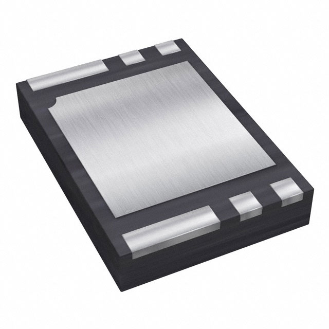
- Part No.:
- AP9214LA-AF-HSB-7
- Manufacturer:
- Diodes Incorporated
- Category:
- Battery Management
- Package:
- 6-UDFN Exposed Pad
- Datasheet:
-
 AP9214LA-AF-HSB-7.pdf
- Description:
- IC BATT PROT LI-ION 1CELL 6UDFN
- Quantity:
- Payment:

- Shipping:

Inventory:2,712
Please send an inquiry. Send us your inquiry, and we will respond immediately.
Product details
Overview
AP9214LA-AF-HSB-7 from Diodes Incorporated is a single-chip Li+ battery protection IC integrating dual N-channel MOSFETs (RSS(ON) ≤ 16 mΩ @ VDD = 4.0V), overcharge/overdischarge voltage detection (±25 mV accuracy), discharge overcurrent sensing (±15 mV), and short-circuit protection with 1 μs response. It operates in 1-cell Li+ packs for portable power tools and medical devices requiring ultra-low quiescent current (3.0 µA typ) and thermal-efficient U-DFN2535-6 (Type B) packaging.
For engineers reviewing the AP9214LA-AF-HSB-7 datasheet, AP9214LA-AF-HSB-7 pinout, AP9214LA-AF-HSB-7 application, or AP9214LA-AF-HSB-7 equivalent, key selection criteria include selectable power-down mode (0.1 µA sleep), 0V battery charge enable, auto-release vs latch overcharge behavior, and dual-pin-option compatibility with PCB layout constraints for VM/S2 routing.
Technical Context
The AP9214LA-AF-HSB-7 implements independent analog comparators for VDD–VSS (cell voltage), VM–VSS (discharge current), and VDD–VM (charge current), each feeding into logic-controlled delay timers (tCU/tDL/tDOC ±20% accuracy). Its internal level-shifted gate drivers directly control two integrated N-MOSFETs sharing a common drain (EP pad), eliminating external FETs and gate resistors.
Protection sequencing is deterministic: overcharge disables only the charging MOSFET (S2), while overdischarge or short-circuit disables only the discharging MOSFET (S1); overvoltage charger detection (8.0 V fixed) independently gates S2. The device supports factory-configured options including 0V charge permission and power-down activation via external charger connection.
Key Specifications
| Parameter | Value and Actual Design Meaning |
|---|---|
| VDD Operating Range | 1.5 V to 5.5 V - supports full Li+ cell voltage range (2.5–4.4 V) plus margin for transient spikes |
| Overcharge Detection Voltage | 4.250 V ±25 mV - factory-trimmed threshold enabling precise termination at standard Li+ upper limit |
| Discharge Overcurrent Threshold | 0.100 V ±15 mV - sets 10 A load cutoff (with 10 mΩ sense path), critical for motor-driven tool safety |
| Quiescent Current (Normal) | 3.0 µA typ @ 3.5 V - extends shelf life of sealed battery packs without compromising responsiveness |
| Short-Circuit Response Time | 1.0 µs typ - prevents catastrophic failure during accidental P+/P− contact in handheld devices |
| MOSFET RSS(ON) | 13 mΩ max @ VDD = 4.0 V - limits I²R loss to <1.2 W at 10 A continuous, enabling compact thermal design |
| Operating Temperature | −40°C to +85°C - qualified for industrial-grade portable equipment with wide ambient exposure |
Pinout & Package
AP9214LA-AF-HSB-7 uses the U-DFN2535-6 (Type B) package with exposed thermal pad (EP), optimized for high-current battery management in space-constrained layouts. Pin-out Option 1 (HSB) places NC on Pin 5 and VM on Pin 4; this variant is used in designs where VM routing to charge path sensing is prioritized.
| Pin/Terminal | Circuit Role | Design Meaning |
|---|---|---|
| S1 | Source of discharge MOSFET | Connects directly to battery negative (P−); switching node for load-side current control |
| VSS | Negative supply reference | System ground return for all internal comparators and logic; must be low-impedance |
| VDD | Positive supply input | Connected to battery positive (P+) via R1 (330–470 Ω); powers internal circuitry and gate drivers |
| VM | Charge/discharge current sense input | Monitors voltage drop across R2 (2.7 kΩ typical) between P− and S2; enables bidirectional current detection |
| NC | No-connect terminal | Pin 5 is unconnected; must remain floating-no trace or solder mask opening required |
| EP | Common drain thermal pad | Shared drain node for both MOSFETs; requires ≥20 mm² copper pour for thermal dissipation and EMI reduction |
Key Features
| Feature | Design Value |
|---|---|
| Integrated dual N-MOSFETs | Eliminates 4 external FETs and gate drive components, reducing BOM count and PCB area by >35% |
| Selectably enabled 0V battery charge | Allows safe reactivation of deeply discharged cells (0 V) using standard CC/CV chargers without manual intervention |
| Configurable overcharge release mode | Factory-set auto-release behavior enables automatic recovery after voltage drops below VCL, avoiding permanent lockout |
| Built-in fixed delay timers | Removes need for external RC networks-tCU = 1.0 s, tDOC = 12 ms, tSHORT = 1.0 µs-ensuring consistent timing across temperature |
| Overvoltage charger detection | Independent 8.0 V (±2 V) monitor between VDD and VM blocks unsafe fast-chargers before they damage the cell |
Applications
| Power Tools | Portable Medical Devices |
|---|---|
|
Use Scenario: Cordless drill/driver battery pack with 10 A peak discharge and frequent deep cycling. IC Role / Device Role / Timing Role: Primary protection controller managing charge/discharge paths, detecting overcurrent during stall conditions within 12 ms. Use Value: Prevents MOSFET thermal runaway during jammed-bit events while maintaining <3 µA self-discharge during storage. |
Use Scenario: Handheld ultrasound probe with sealed 3.7 V Li+ cell requiring FDA-compliant safety redundancy. IC Role / Device Role / Timing Role: Standalone hardware-level protector enforcing strict voltage windows (2.5–4.3 V) and disabling output on 1 µs short detection. Use Value: Meets IEC 62304 Class C requirements without software supervision-guaranteed fail-safe shutdown. |
| Wearable Fitness Trackers | Smart Home Sensors |
|
Use Scenario: Slim wrist-worn tracker with 120 mAh cell and aggressive power budgeting. IC Role / Device Role / Timing Role: Low-quiescent supervisor enabling 5-year shelf life; activates 0V charge function to recover after long-term storage. Use Value: Eliminates field returns due to "dead battery" syndrome-users recharge successfully even after 2+ years idle. |
Use Scenario: Battery-powered CO detector deployed in unconditioned attics (-25°C to +70°C). IC Role / Device Role / Timing Role: Ambient-robust protector validating cell voltage at −40°C and rejecting false trips from cold-temperature hysteresis drift. Use Value: Maintains ±35 mV overdischarge accuracy across full spec temp range-prevents premature shutdown in winter installations. |
Equivalent & Alternatives
The following parts are listed as comparable options for similar 1-cell Li+ battery protection applications.
| Alternative Part | Technical Difference | Application Difference | Selection Advice |
|---|---|---|---|
| Seiko Instruments S-8261AAL-M6T1U | Single-MOSFET architecture; no integrated charge MOSFET; requires external P-FET for charge path | Lacks bidirectional current sensing-cannot detect charge overcurrent or support 0V charge | Choose only if cost sensitivity outweighs functional completeness and board space is unconstrained |
| Ricoh RP502K001A-TR-F | Higher quiescent current (12 µA typ); no overvoltage charger detection; fixed 2.5 V overdischarge threshold | Not suitable for high-accuracy chemistries (e.g., LiFePO₄ blends) or fast-charger environments | Select when legacy design reuse is mandatory and thermal performance is secondary to procurement continuity |
Compared with S-8261AAL-M6T1U and RP502K001A-TR-F, the AP9214LA-AF-HSB-7 delivers full bidirectional protection in one die, reduces system-level component count by ≥6, and enables safer operation with fast-charger compatibility and sub-µs fault response-critical for premium portable electronics.
Availability
AP9214LA-AF-HSB-7 is available at Aetrix Electronics and suitable for power tools, portable medical devices, wearables, and smart home sensors requiring stable component supply, long-term lifecycle assurance, and RoHS-compliant manufacturing.
Supply support for AP9214LA-AF-HSB-7 includes scheduled delivery planning, volume procurement assistance, BOM continuity management, traceable sourcing, and lifecycle availability coordination for OEM customers, industrial embedded developers, connected-device designers, and electronics production programs.
Manufacturer
Diodes Incorporated is a global semiconductor manufacturer specializing in discrete, analog, and mixed-signal solutions for power management, signal integrity, and protection applications.
The AP9214L series targets compact, high-reliability Li+ battery packs in consumer and industrial markets, emphasizing integration density, ultra-low power, and factory-programmable safety features without external configuration.
FAQ
What is the function of the NC pin on AP9214LA-AF-HSB-7?
Pin 5 is designated NC (No Connect) in the HSB pin-out option and must remain electrically floating-no trace, solder mask opening, or thermal connection is permitted. This pin has no internal bond wire and serves solely as a mechanical alignment marker for automated placement. Connecting it risks latch-up or undefined logic states due to parasitic coupling.
How does the 0V battery charge feature operate in practice?
When enabled, the AP9214LA-AF-HSB-7 allows charging current to flow into a fully depleted (0 V) cell by temporarily bypassing the overdischarge lockout. It monitors rising voltage and engages normal protection once VDD exceeds 1.2 V. This occurs without user intervention and is validated down to −40°C, making it ideal for infrequently used backup devices.
Can AP9214LA-AF-HSB-7 support both charge and discharge overcurrent protection simultaneously?
No-it provides separate, mutually exclusive overcurrent paths: discharge overcurrent (VM–VSS ≥ 0.100 V) triggers S1 shutdown, while charge overcurrent (VM–VSS ≤ −0.100 V) triggers S2 shutdown. The device cannot detect simultaneous opposing currents because VM is a single-ended sense node referenced to VSS, not a differential input.
What thermal design guidance applies to the EP pad?
The EP pad is the common drain for both MOSFETs and must be connected to ≥20 mm² of 2-ounce copper with ≥4 thermal vias (0.3 mm diameter) to an internal ground plane. Without this, junction temperature exceeds 150°C at 7 A continuous, violating absolute maximum ratings and triggering thermal shutdown.
AP9214LA-AF-HSB-7 Specifications
- Product attributes
- Attribute value
- Manufacturer:
- Diodes Incorporated
- Series:
- -
- Package/Case:
- 6-UDFN Exposed Pad
- Packaging:
- Tape & Reel (TR)
- Product Status:
- Active
- Function:
- Battery Protection
- Battery Chemistry:
- Lithium Ion/Polymer
- Number of Cells:
- 1
- Fault Protection:
- Over Current, Over Voltage, Short Circuit
- Interface:
- -
- Operating Temperature:
- -40°C ~ 85°C (TA)
- Grade:
- -
- Qualification:
- -
- Mounting Type:
- Surface Mount
- Supplier Device Package:
- U-DFN2535-6
AP9214LA-AF-HSB-7 FAQ
1.How can I place an order for AP9214LA-AF-HSB-7 through Aetrix?
Please submit a Request for Quotation (RFQ) for AP9214LA-AF-HSB-7 on Aetrix. Our sales agent will provide a competitive quotation and guide you through the order confirmation once you accept the terms.
2.Are the price and stock information for AP9214LA-AF-HSB-7 reliable?
The price and inventory of AP9214LA-AF-HSB-7 are updated periodically and may fluctuate due to market conditions. Stock and pricing data are typically refreshed every 24 hours. Quotation validity for AP9214LA-AF-HSB-7 is usually 5 days.
3.What payment methods are accepted for AP9214LA-AF-HSB-7?
We accept Wire Transfer, PayPal, Credit Card, Western Union, MoneyGram, and Escrow for AP9214LA-AF-HSB-7 transactions.
Note: Certain payment methods may incur a processing fee.
4.How is shipping managed for AP9214LA-AF-HSB-7?
AP9214LA-AF-HSB-7 orders can be shipped via leading logistics carriers, including DHL, UPS, FedEx, TNT, or Registered Mail.
Once your AP9214LA-AF-HSB-7 order is processed, you will receive an email with the shipment details and tracking number.
Note: Tracking information may take up to 24 hours to appear. Express delivery typically takes 3–5 business days.
5.How can I obtain technical support or documentation for AP9214LA-AF-HSB-7?
For technical support, including AP9214LA-AF-HSB-7 datasheets, pinout diagrams, or application guidance, please contact our engineering support team. They can provide detailed documentation and assistance for your AP9214LA-AF-HSB-7 requirements.
6.How does Aetrix verify that AP9214LA-AF-HSB-7 is sourced from the original manufacturer or authorized distributors?
All AP9214LA-AF-HSB-7 products on Aetrix are procured from qualified distributors and authorized channels. Our dedicated quality assurance team conducts strict verification, including traceability checks and, if necessary, third-party testing. This ensures that AP9214LA-AF-HSB-7 meets industry standards.
7.What is the process for return or replacement of AP9214LA-AF-HSB-7?
All AP9214LA-AF-HSB-7 units undergo pre-shipment inspection (PSI). If there is an issue with AP9214LA-AF-HSB-7, returns or replacements are accepted under the following conditions:
1.Quantity discrepancies, incorrect items, or visible external defects (such as breakage or corrosion), acknowledged by Aetrix.
2.The issue is reported within 90 days of delivery.
3.The AP9214LA-AF-HSB-7 part is unused and in its original packaging.
Return procedure for AP9214LA-AF-HSB-7:
1.Submit a request within 90 days.
2.Obtain a Return Material Authorization (RMA) from Aetrix.
AP9214LA-AF-HSB-7 Tags

-
BQ29700DSER
Texas Instruments

-
S-8241ABKMC-GBKT2G
ABLIC Inc.
-
S-8241ABPMC-GBPT2G
ABLIC Inc.

-
BQ27427YZFR
Texas Instruments

-
BQ27426YZFR
Texas Instruments

-
STC3117IJT
STMicroelectronics

-
STC3115IJT
STMicroelectronics

-
BQ76925RGER
Texas Instruments
-
NPM1100-QDAA-R
Nordic Semiconductor ASA

-
BQ27441DRZR-G1A
Texas Instruments

-
STC3115AIQT
STMicroelectronics

-
S-8252AAL-M6T1U
ABLIC Inc.
Tech Hub

An engineering guide to LED driver operation, constant-current and constant-voltage outputs, linear and switching topologies, dimming, IC selection, calculations, replacement compatibility, and fault c…

Operational amplifier guide covering op amp basics, feedback, ideal vs real op amps, common configurations, buffer circuits, offset, bias current, gain-bandwidth, slew rate, rail-to-rail limits and sel…

Jumper cables guide covering safe connection order, red and black clamp placement, final ground connection, cable gauge, length, clamp quality, copper vs CCA cables, jump starter comparison and battery…

LDO regulator guide covering low dropout voltage, power dissipation, thermal design, PSRR, output noise, capacitor stability, adjustable LDO circuits, LDO vs buck converter and datasheet selection chec…

Conditional Access Module guide covering CAM meaning, CI/CI+ interface, smart card authorization, DVB security workflow, TV and set-top box compatibility, internal electronics, ESD protection, connecto…

Guide to electronic component obsolescence covering EOL risk, PCN/PDN notices, last-time buy planning, replacement options, form-fit-function validation, counterfeit risk and BOM lifecycle management.

18650 battery guide covering lithium-ion cell basics, 3.6V/3.7V voltage, 4.2V charging, mAh and Wh capacity, protected cells, chargers, BMS, series-parallel packs, holders, welding and sourcing checks.…

Hall effect sensor guide covering working principle, linear and digital sensors, Arduino circuits, current sensing, speed detection, automotive applications, A3144 examples, signal filtering and datash…

Product Change Notification guide for electronic components, covering PCN meaning, PCN vs PDN/EOL, common change types, risk levels, form-fit-function review, engineering validation, BOM control, LTB/L…

A practical guide to blend door actuators, covering HVAC function, symptoms, location, AC and heater issues, reset and calibration, replacement cost, electrical diagnosis, compatibility checks, and rep…


