
 My Inquiry
 My Account


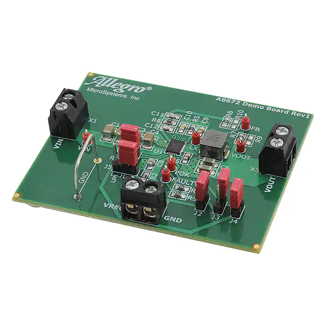
Allegro MicroSystems APEK8672EEG-01-T-DK
- Part No.:
- APEK8672EEG-01-T-DK
- Manufacturer:
- Allegro MicroSystems
- Package:
- Datasheet:
-
 APEK8672EEG-01-T-DK.pdf
- Description:
- EVAL BOARD FOR A8672
- Quantity:
- Payment:

- Shipping:

Inventory:3,299
Please send an inquiry. Send us your inquiry, and we will respond immediately.
Product details
Overview
APEK8672EEG-01-T-DK from Allegro MicroSystems is a discontinued fixed-frequency synchronous buck regulator delivering up to 8 A, featuring valley current mode control, 0.6 V adjustable output, integrated 5 V LDO, and dual fault reporting (FAULT/POK) for server point-of-load applications.
For engineers reviewing the APEK8672EEG-01-T-DK datasheet, APEK8672EEG-01-T-DK pinout, APEK8672EEG-01-T-DK application, or APEK8672EEG-01-T-DK equivalent, this page provides verified technical context, validated pin functions, confirmed thermal and electrical specifications, and real-world design constraints for legacy system support and obsolescence mitigation.
Technical Context
The APEK8672EEG-01-T-DK implements valley current mode control with voltage feedforward and frequency modulation during load transients, enabling ultra-fast response and stable operation at high switching frequencies (200–1000 kHz). Its architecture integrates high-side (27 mΩ) and low-side (12 mΩ) MOSFETs with programmable on-time via external resistor on TON pin.
It supports dual operating modes-fixed continuous conduction mode (FCCM) and low-power mode (LPM)-selected via MODE pin, and includes comprehensive protection: thermal shutdown (165°C), overtemperature fault (140°C), output overvoltage (115–125% VFB), undervoltage (75% VFB), and LX short-to-ground detection.
Key Specifications
| Parameter | Value and Actual Design Meaning |
|---|---|
| Output Current | Up to 8 A continuous; enables high-density point-of-load conversion in space-constrained server boards. |
| Input Voltage Range | 3–16 V power input; supports 5 V, 12 V, and intermediate bus architectures without external regulators. |
| Output Voltage Range | Adjustable down to 0.6 V ±1% reference accuracy; meets core voltage requirements for modern CPUs/FPGAs. |
| Switching Frequency | 200–1000 kHz programmable; balances efficiency, EMI, and component size for telecom and storage systems. |
| On-Resistance | 27 mΩ (HS), 12 mΩ (LS); reduces conduction loss and improves full-load efficiency above 90% at 12 V → 1.2 V. |
| Fault Reporting | Dedicated open-drain FAULT (thermal/LX short) and POK (output regulation) pins; enables host-level system health monitoring. |
| Thermal Resistance | RθJA = 33 °C/W (4-layer PCB); requires exposed pad soldering and thermal vias for safe 8 A operation at 85°C ambient. |
Pinout & Package
The APEK8672EEG-01-T-DK uses a 28-contact, 4 mm × 5 mm, 0.75 mm nominal height QFN package with exposed thermal pad (EG suffix), Pb-free with 100% matte tin plating.
| Pin/Terminal | Circuit Role | Design Meaning |
|---|---|---|
| AGND | Analog ground reference | Must connect to PGND at PAD; serves as FB divider ground for ±1% output accuracy. |
| PGND (Pins 2–6) | Power ground return path | Low-impedance connection to exposed pad; carries high ripple current from LX node. |
| VIN (Pins 7–8) | Main power input | Bypassed locally with ≥22 µF ceramic; supplies high-side MOSFET drain and input filter network. |
| VDD (Pin 9) | Control circuit supply | Can be tied to VIN or driven separately; ensures gate drive strength across 4.5–16 V control range. |
| TON (Pin 10) | On-time programming | Resistor between TON and VIN sets switching frequency; tolerance ±10% affects fSW stability. |
| VREG (Pin 11) | 5 V LDO output | Supplies internal bias and external MODE/ILIM circuits; delivers 0–30 mA with ±5% regulation. |
| FAULT (Pin 12) | Open-drain fault indicator | Pulled low on thermal shutdown (>140°C), LX short, or timing resistor open; requires external pull-up. |
| POK (Pin 13) | Open-drain power-good | Asserts low after 90 µs delay when VOUT reaches 92–98% of target; excludes thermal faults. |
| EN (Pin 14) | Enable logic input | Active-high with 1.8 V threshold and 250 mV hysteresis; controls startup sequencing and standby entry. |
| BOOT (Pin 15) | High-side gate drive supply | Connected to LX via 2.2 µF capacitor; critical for proper high-side MOSFET turn-on and shoot-through prevention. |
| LX (Pins 16–22) | Switch node | Connects to inductor and BOOT cap; handles full switching current; must minimize loop area for EMI control. |
| BIAS (Pin 23) | Internal bias regulator output | Stabilizes gate drive and control circuits; bypassed with 470 nF ceramic per datasheet layout guidelines. |
| MODE (Pin 24) | Operating mode select | Pull to VREG for FCCM (full-load efficiency); tie to GND for LPM (light-load quiescent current reduction). |
| ILIM (Pin 25) | Valley current limit set | Resistor to GND programs 3–10 A limit; enables inductor sizing without oversizing for fault currents. |
| SS (Pin 26) | Soft-start ramp control | Capacitor defines rise time and hiccup shutdown period; prevents inrush and output overshoot. |
| COMP (Pin 27) | Error amplifier compensation | Connect R-C network to AGND; determines loop stability and transient recovery behavior. |
| FB (Pin 28) | Feedback voltage sense | Monitors output via resistor divider; triggers POK, UV/OV faults, and regulates VOUT to 0.6 V reference. |
| PAD | Exposed thermal/electrical pad | Must be soldered to PCB ground plane with ≥6 thermal vias; primary path for heat dissipation and PGND return. |
Key Features
| Feature | Design Value |
|---|---|
| Valley current mode control | Enables <50 ns minimum on-time and stable 12 V → 0.6 V conversion at >1 MHz without sub-harmonic oscillation. |
| Programmable pulse-by-pulse current limit | Eliminates need for oversized inductors by limiting peak current per cycle during overload, reducing thermal stress. |
| Integrated 5 V LDO (VREG) | Provides regulated bias for MODE, ILIM, and external circuitry; eliminates need for separate LDO in compact designs. |
| Ultra-fast transient response | Combines voltage feedforward and frequency modulation to maintain regulation during >2 A/µs load steps in server applications. |
| Comprehensive fault reporting | Separate FAULT (thermal/LX short) and POK (output regulation) outputs allow independent host-system diagnostics and graceful shutdown. |
Applications
| Server CPU Core Supply | Network ASIC Point-of-Load |
|---|---|
Use Scenario: Delivering tightly regulated 0.8–1.2 V at up to 8 A to multi-core processors in 1U rack servers. IC Role / Device Role / Timing Role: Primary synchronous buck regulator with valley current mode control and fast transient response. Use Value: Maintains output within ±1% during rapid load steps while minimizing output capacitance and board area. | Use Scenario: Powering high-speed SerDes and packet processing units in 10/25/100 GbE switches and routers. IC Role / Device Role / Timing Role: Fixed-frequency buck converter with programmable soft-start and hiccup shutdown for reliable hot-swap operation. Use Value: Prevents bus collapse during insertion by limiting inrush and detecting overcurrent before damage occurs. |
| Enterprise Storage Controller | Industrial FPGA I/O Bank Supply |
Use Scenario: Generating 1.8 V or 2.5 V for NVMe SSD controllers and RAID ASICs in enterprise storage arrays. IC Role / Device Role / Timing Role: High-efficiency buck regulator with 5 V LDO for auxiliary bias and fault-aware power sequencing. Use Value: Reduces thermal load in sealed enclosures via 33 °C/W RθJA and enables predictive maintenance using FAULT/POK status. | Use Scenario: Providing configurable 1.2–3.3 V supplies to FPGA I/O banks in programmable logic controllers and test equipment. IC Role / Device Role / Timing Role: Adjustable-output buck with precise ±1% reference and programmable current limit for mixed-voltage I/O domains. Use Value: Ensures signal integrity by maintaining tight voltage tolerance across temperature and load variations. |
Equivalent & Alternatives
The following parts are listed as comparable options for similar synchronous buck regulator applications.
| Alternative Part | Technical Difference | Application Difference | Selection Advice |
|---|---|---|---|
| MP2451DT-LF-Z | 36 V max input, 0.8 A output, no integrated fault reporting or POK; requires external current sense. | Suitable only for low-current industrial sensors-not a functional replacement for 8 A server loads. | Select only if input voltage exceeds 16 V and output current ≤0.8 A; verify thermal derating on 4-layer PCB. |
| TPS54821RHLR | 6 A max output, 4.5–20 V input, integrated PMBus interface, but no valley current mode or dedicated FAULT pin. | Supports digital telemetry in data center PSUs but lacks analog fault signaling required for legacy server BMCs. | Use where telemetry and remote configuration are prioritized over analog fault flag compatibility with existing firmware. |
Compared with APEK8672EEG-01-T-DK, MP2451DT-LF-Z offers higher input voltage tolerance but cannot meet the 8 A output or FAULT/POK signaling requirements, while TPS54821RHLR provides digital control and margining at the cost of analog fault visibility and reduced current capability-neither is a drop-in replacement.
Availability
APEK8672EEG-01-T-DK is available at Aetrix Electronics and suitable for server power delivery, network point-of-load, and enterprise storage applications requiring stable component supply despite end-of-life status.
Supply support for APEK8672EEG-01-T-DK includes scheduled delivery planning, volume procurement assistance, BOM continuity management, traceable sourcing, and lifecycle availability coordination for OEM customers, industrial embedded developers, connected-device designers, and electronics production programs.
Manufacturer
Allegro MicroSystems is a U.S.-based designer of high-performance power ICs and magnetic sensors, headquartered in Manchester, NH, with focus on automotive, industrial, and computing power solutions.
The APEK8672EEG-01-T-DK belongs to Allegro's high-current synchronous buck regulator product line, engineered specifically for high-efficiency, fault-aware DC/DC conversion in space- and thermally-constrained computing infrastructure.
FAQ
Is APEK8672EEG-01-T-DK still in production?
No, APEK8672EEG-01-T-DK is a discontinued product. Allegro MicroSystems ceased production effective September 1, 2016. It is not recommended for new designs, and samples are no longer available. Aetrix Electronics maintains limited legacy stock for repair and continuity support under controlled allocation.
What does the "-DK" suffix indicate in APEK8672EEG-01-T-DK?
The "-DK" suffix denotes a specific tape-and-reel packaging variant used for distribution through authorized channels. It does not reflect a functional or electrical difference from the base A8672EEGTR-T part-it shares identical silicon, pinout, and specifications with the standard EG-package version.
Can APEK8672EEG-01-T-DK operate with a 3.3 V input?
Yes, APEK8672EEG-01-T-DK supports a minimum 3 V power input voltage. However, its control circuitry requires VDD ≥4.5 V; therefore, VDD must be supplied externally (e.g., from a separate 5 V rail) when VIN is below 4.5 V to ensure proper gate drive and regulation.
How is the switching frequency set on APEK8672EEG-01-T-DK?
The switching frequency of APEK8672EEG-01-T-DK is set by an external resistor (RTON) connected between the TON pin and VIN. For example, a 90.9 kΩ resistor yields ~500 kHz at 12 V input and 1.2 V output. The on-time tolerance is ±10%, and frequency varies with input/output voltage due to valley current mode operation.
Does APEK8672EEG-01-T-DK require external MOSFETs?
No, APEK8672EEG-01-T-DK integrates both high-side (27 mΩ) and low-side (12 mΩ) power MOSFETs. No external switches are needed-only passive components (inductor, input/output capacitors, feedback resistors, BOOT capacitor, and optional SS/ILIM/TON resistors) are required for full operation.
APEK8672EEG-01-T-DK Specifications
- Product attributes
- Attribute value
- Manufacturer:
- Allegro MicroSystems
- Series:
- -
- Packaging:
- Bulk
- Product Status:
- Obsolete
- Main Purpose:
- DC/DC, Step Down with LDO
- Outputs and Type:
- 2 Non-Isolated Outputs
- Voltage - Output:
- -
- Current - Output:
- -
- Voltage - Input:
- 8A, 30mA
- Regulator Topology:
- 3V ~ 16V
- Frequency - Switching:
- Buck
- Contents:
- -
- Utilized IC / Part:
- Board(s)
- Power - Output:
- A8672
APEK8672EEG-01-T-DK FAQ
1.How can I place an order for APEK8672EEG-01-T-DK through Aetrix?
Please submit a Request for Quotation (RFQ) for APEK8672EEG-01-T-DK on Aetrix. Our sales agent will provide a competitive quotation and guide you through the order confirmation once you accept the terms.
2.Are the price and stock information for APEK8672EEG-01-T-DK reliable?
The price and inventory of APEK8672EEG-01-T-DK are updated periodically and may fluctuate due to market conditions. Stock and pricing data are typically refreshed every 24 hours. Quotation validity for APEK8672EEG-01-T-DK is usually 5 days.
3.What payment methods are accepted for APEK8672EEG-01-T-DK?
We accept Wire Transfer, PayPal, Credit Card, Western Union, MoneyGram, and Escrow for APEK8672EEG-01-T-DK transactions.
Note: Certain payment methods may incur a processing fee.
4.How is shipping managed for APEK8672EEG-01-T-DK?
APEK8672EEG-01-T-DK orders can be shipped via leading logistics carriers, including DHL, UPS, FedEx, TNT, or Registered Mail.
Once your APEK8672EEG-01-T-DK order is processed, you will receive an email with the shipment details and tracking number.
Note: Tracking information may take up to 24 hours to appear. Express delivery typically takes 3–5 business days.
5.How can I obtain technical support or documentation for APEK8672EEG-01-T-DK?
For technical support, including APEK8672EEG-01-T-DK datasheets, pinout diagrams, or application guidance, please contact our engineering support team. They can provide detailed documentation and assistance for your APEK8672EEG-01-T-DK requirements.
6.How does Aetrix verify that APEK8672EEG-01-T-DK is sourced from the original manufacturer or authorized distributors?
All APEK8672EEG-01-T-DK products on Aetrix are procured from qualified distributors and authorized channels. Our dedicated quality assurance team conducts strict verification, including traceability checks and, if necessary, third-party testing. This ensures that APEK8672EEG-01-T-DK meets industry standards.
7.What is the process for return or replacement of APEK8672EEG-01-T-DK?
All APEK8672EEG-01-T-DK units undergo pre-shipment inspection (PSI). If there is an issue with APEK8672EEG-01-T-DK, returns or replacements are accepted under the following conditions:
1.Quantity discrepancies, incorrect items, or visible external defects (such as breakage or corrosion), acknowledged by Aetrix.
2.The issue is reported within 90 days of delivery.
3.The APEK8672EEG-01-T-DK part is unused and in its original packaging.
Return procedure for APEK8672EEG-01-T-DK:
1.Submit a request within 90 days.
2.Obtain a Return Material Authorization (RMA) from Aetrix.
APEK8672EEG-01-T-DK Tags
-
DFR0571
DFRobot
-
DFR0379
DFRobot
-
DFR0205
DFRobot
-
1385
Adafruit Industries LLC
-
COM-15208
SparkFun Electronics
-
1944
Adafruit Industries LLC
-
2465
Adafruit Industries LLC
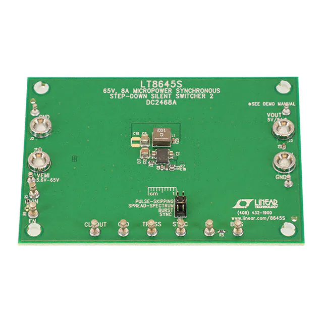
-
DC2468A
Analog Devices Inc.
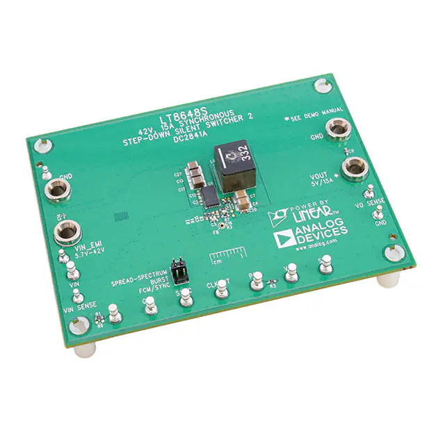
-
DC2841A
Analog Devices Inc.

-
TPS552892EVM-111
Texas Instruments
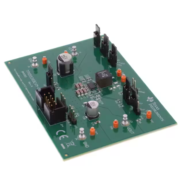
-
TPS55289EVM-093
Texas Instruments
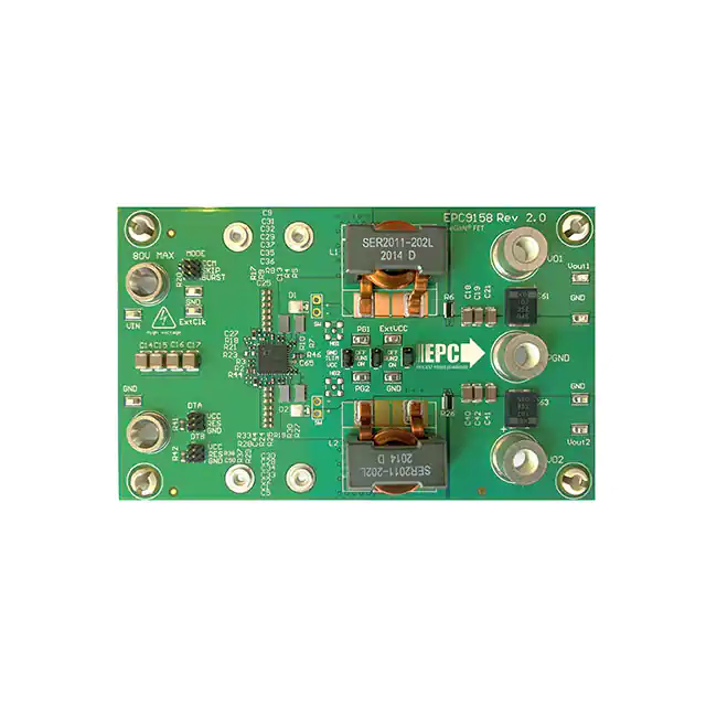
-
EPC9158
EPC
Tech Hub

A practical engineering and sourcing framework covering lifecycle verification, lifetime-buy calculations, replacement qualification, supplier checks and counterfeit-risk controls.

TTL and CMOS logic families differ in thresholds, loading, output drive, power and timing. This engineering guide compares 74HC and 74HCT, calculates noise margins and checks 3.3 V/5 V compatibility.

A practical engineering guide to 3.3V and 5V logic compatibility, input thresholds, resistor dividers, translator ICs, MOSFET level shifting, I2C pull-ups, timing limits and power-sequencing risks.

The 74HC595 uses push-pull logic outputs, while the TPIC6B595 uses 50 V open-drain DMOS sinks for higher-power loads. This guide compares timing, current limits, 3.3 V interfacing, load wiring, thermal…

The 74HC595 converts serial data into eight stable parallel outputs. This guide covers pin functions, shift and storage timing, OE and MR behavior, drive-current limits, cascading, voltage compatibilit…

A technical comparison of level-sensitive latches and edge-triggered flip-flops, covering timing windows, setup and hold limits, master–slave operation, time borrowing, race-through, HDL inference and…

A D latch stores one bit while Enable controls when data can pass. This reference covers gate-level operation, truth tables, transparency, setup and hold timing, LE versus OE, common ICs and practical …

An SR latch stores one bit through cross-coupled feedback. This engineering reference covers NOR and NAND implementations, truth tables, forbidden-state recovery, gated operation, switch debouncing, fa…

Latch circuits retain one bit through feedback. This technical reference covers SR and D latches, truth tables, transparency, timing limits, latch-versus-flip-flop behavior, applications and common log…

An engineering guide to LED driver operation, constant-current and constant-voltage outputs, linear and switching topologies, dimming, IC selection, calculations, replacement compatibility, and fault c…


