
 My Inquiry
 My Account


Diodes Incorporated APR34309CMPTR-G1
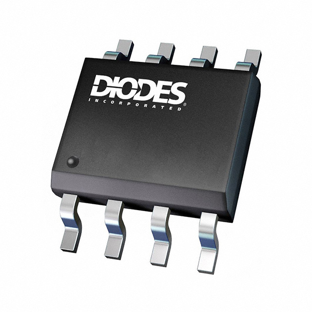
- Part No.:
- APR34309CMPTR-G1
- Manufacturer:
- Diodes Incorporated
- Category:
- Power Supply Controllers, Monitors
- Package:
- 8-SOIC (0.154", 3.90mm Width) Exposed Pad
- Datasheet:
-
 APR34309CMPTR-G1.pdf
- Description:
- ACDC SYNCH RECT CONT 8-SO
- Quantity:
- Payment:

- Shipping:

Inventory:1,338
Please send an inquiry. Send us your inquiry, and we will respond immediately.
Product details
Overview
APR34309CMPTR-G1 from Diodes Incorporated is a secondary-side synchronous rectification (SR) Combo IC integrating an N-channel MOSFET and driver for DCM-mode flyback converters. It features 8 mΩ RDS(ON) at VGS = 4.5 V, 20 A continuous drain current, and output voltage detect functionality with 5.15 V internal trigger voltage. It enables high-efficiency 5 V output adapters by replacing Schottky diodes in low-voltage, high-current secondary-side rectification.
For engineers reviewing the APR34309CMPTR-G1 datasheet, APR34309CMPTR-G1 pinout, APR34309CMPTR-G1 application, or APR34309CMPTR-G1 equivalent, key selection criteria include SR timing accuracy (tDON = 70–130 ns), volt-second product detection via AREF resistor programming, integrated OVP discharge (IOVP = 40–100 mA), and SO-8EP thermal performance (θJA = 56 °C/W).
Technical Context
The APR34309C implements a dual-function architecture: a fast-turning SR driver triggered by drain-to-source voltage sensing (VTHOFF = −13 to −5 mV), and a dynamic output voltage monitor that generates periodic pulses at VDET when VCC < VTRIGGER (5.15 V typ), then activates OVP discharge above VDIS = 5.3 V. Its minimum on-time blanking logic uses (VDET−VCC)×tONP integration to reject primary-side ringing interference.
It operates exclusively in discontinuous conduction mode (DCM) flyback topologies, where SR turn-off timing directly impacts PSR feedback stability. The device's gate drive rise/fall times (tRG/tFG = 50–100 ns) and body-diode reverse recovery optimization ensure minimal conduction loss and zero-crossing detection fidelity without external snubbers.
Key Specifications
| Parameter | Value and Actual Design Meaning |
|---|---|
| RDS(ON) | 8 mΩ max at VGS = 4.5 V - enables <150 mW conduction loss at 5 V/3 A output. |
| VTRIGGER | 5.15 V typical - sets precise threshold for disabling VDET pulsing and enabling stable regulation. |
| tDON/tDOFF | 70–130 ns / 100–150 ns - ensures sub-150 ns SR switching alignment with secondary current zero-crossing. |
| VTHOFF | −13 to −5 mV - ultra-low negative threshold rejects noise while enabling early turn-off before reverse conduction. |
| IOVP | 40–100 mA - delivers controlled discharge current to clamp overshoot during load transients. |
| θJA | 56 °C/W - supports 2.2 W power dissipation on standard FR-4 PCB with 1 in² copper pad. |
| Kqs | 0.325–0.515 mA·μs - defines AREF resistor value for volt-second product threshold calibration. |
Pinout & Package
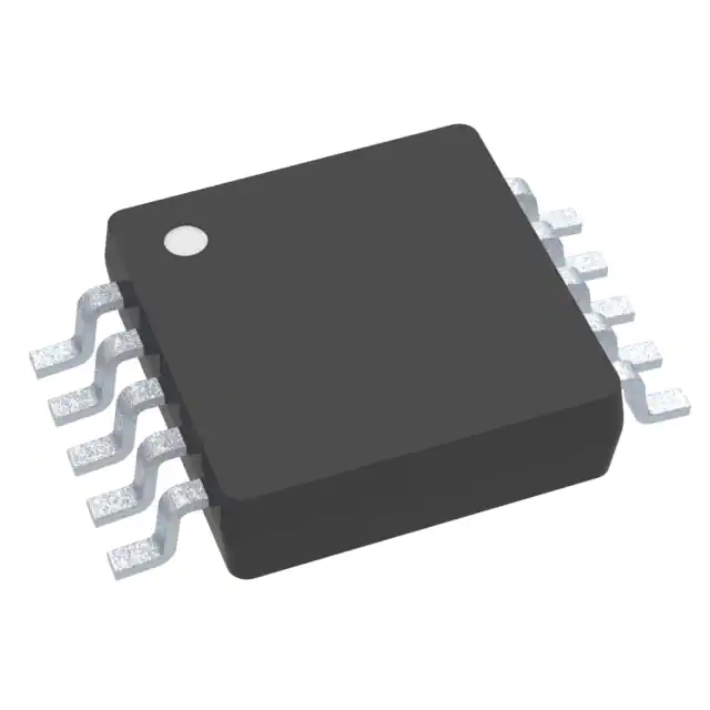
APR34309CMPTR-G1 is housed in an SO-8EP package with exposed drain pad (EP) for thermal and current handling. The 8-pin layout includes three GND pins (6, 7, 8) tied to MOSFET source, and the EP serves as the high-current drain return path. Thermal resistance θJC = 12 °C/W confirms direct junction-to-case heat transfer through the exposed pad.
| Pin/Terminal | Circuit Role | Design Meaning |
|---|---|---|
| 1 DRISR | SR gate drive output | Active-high MOSFET gate signal with 3.7 V min high-level drive at VCC = 5 V. |
| 2 VDET | SR sense & dynamic function I/O | Senses drain voltage; outputs periodic pulse when VCC < VTRIGGER; connects to DRAIN via resistor. |
| 3 AREF | Volt-second product reference input | Programs SR activation threshold via external resistor; Kqs × RAREF sets integration boundary. |
| 4 VCC | Supply input & OVP sense node | Powered from 5 V output rail; monitors for UVLO (2.8 V) and OVP (5.74 V); sinks IOVP discharge current. |
| 5 DRAIN | MOSFET drain terminal | Internal N-MOSFET drain connection; routed to exposed pad; carries full secondary current. |
| 6,7,8 GND | MOSFET source & IC ground | Common source node for internal MOSFET; low-inductance return path for SR current and control circuitry. |
Key Features
| Feature | Design Value |
|---|---|
| Integrated SR driver + MOSFET | Eliminates discrete gate driver and external MOSFET, reducing BOM count and layout area in 5 V adapter designs. |
| Volt-second product detection | Rejects primary-side ringing interference using (VDET−VCC)×tONP integration, preventing false SR turn-on in DCM flyback. |
| OVP/UVLO with discharge current | Provides active clamping via programmable IOVP (40–100 mA) and tOVP_LAST = 2.0 ms, improving transient response over passive Zener solutions. |
| Fast SR timing control | Sub-150 ns propagation delays and 50 ns gate edge rates enable accurate zero-current switching in high-frequency DCM converters. |
| SO-8EP thermal design | Exposed drain pad delivers 12 °C/W junction-to-case thermal resistance, supporting 20 A continuous current with minimal heatsinking. |
Applications
| USB-C PD Adapters | 5 V Auxiliary Power Supplies |
|---|---|
|
Use Scenario: 5 V/3 A USB-C power adapter using DCM flyback with primary-side regulation (PSR). IC Role / Device Role / Timing Role: Secondary-side synchronous rectifier controller and MOSFET, providing gate drive synchronized to secondary current zero-crossing. Use Value: Reduces rectifier loss by >40% vs. Schottky diode, enabling >92% efficiency at full load and eliminating heatsink requirements. |
Use Scenario: Standby auxiliary supply in industrial PLCs delivering regulated 5 V to microcontrollers and sensors. IC Role / Device Role / Timing Role: SR switcher with integrated OVP discharge, ensuring stable 5 V output during line surges and load transients. Use Value: Maintains regulation within ±1% during 100 ms 20% line step changes, thanks to fast VDET response (<30 μs) and dynamic OVP clamping. |
| Wireless Phone Chargers | DSL/ADSL Modem Power |
|
Use Scenario: Compact 5 V wireless charging base station with space-constrained PCB layout. IC Role / Device Role / Timing Role: Combo IC combining SR MOSFET and driver in single SO-8EP footprint, minimizing trace inductance and EMI. Use Value: Enables 12 mm × 12 mm secondary-side layout with <5 mV output ripple due to low RDS(ON) and fast switching. |
Use Scenario: Low-noise 5 V power rail for ADSL line drivers and analog front-end circuits. IC Role / Device Role / Timing Role: Synchronous rectifier with ultra-low VTHOFF (−9 mV typ) to minimize body diode conduction time and associated noise. Use Value: Reduces switching noise floor by 12 dB compared to diode rectification, meeting DSL spectral mask requirements. |
Equivalent & Alternatives
The following parts are listed as comparable options for similar synchronous rectification applications.
| Alternative Part | Technical Difference | Application Difference | Selection Advice |
|---|---|---|---|
| APR34308CMPTR-G1 | Same SO-8EP package but lower 12 mΩ RDS(ON), no OVP discharge function, fixed VTRIGGER = 4.9 V. | Lacks active OVP clamping; suitable only for systems with external overvoltage protection. | Select when cost sensitivity outweighs need for integrated OVP and higher efficiency is not required. |
| MP6908AGS-Z | Higher 15 mΩ RDS(ON), 30 V VDSS, no integrated MOSFET - requires external FET; supports CCM/DCM. | Requires external MOSFET and gate resistor tuning; broader topology support but larger solution size. | Select when CCM operation or higher breakdown voltage (>50 V) is needed, accepting added component count. |
Compared with APR34308CMPTR-G1, APR34309CMPTR-G1 adds OVP discharge and lowers RDS(ON) for better efficiency; versus MP6908AGS-Z, it trades topology flexibility for smaller footprint and lower system-level BOM cost in DCM 5 V adapters.
Availability
APR34309CMPTR-G1 is available at Aetrix Electronics and suitable for USB-C PD adapters, DSL modem power supplies, wireless charging bases, and industrial auxiliary rails requiring stable component supply across production lifecycles.
Supply support for APR34309CMPTR-G1 includes scheduled delivery planning, volume procurement assistance, BOM continuity management, traceable sourcing, and lifecycle availability coordination for OEM customers, industrial embedded developers, connected-device designers, and electronics production programs.
Manufacturer
Diodes Incorporated is a global manufacturer of discrete semiconductors and analog ICs, specializing in power management, signal integrity, and protection solutions for high-volume consumer and industrial markets.
The APR34309C belongs to Diodes' secondary-side SR controller product line, engineered specifically for high-efficiency, low-component-count DCM flyback converters targeting 5 V output portable and network power applications.
FAQ
What is the purpose of the AREF pin and how is its resistor value determined?
The AREF pin sets the volt-second product threshold for synchronous rectifier activation using an external resistor. Its value is calculated via Kqs × RAREF = (VDET−VCC)×tONP, where Kqs ranges from 0.325 to 0.515 mA·μs. Designers select RAREF to ensure the integrated area exceeds ringing-induced false triggers while remaining below the true flyback conduction event.
How does APR34309CMPTR-G1 handle primary-side ringing interference during DCM operation?
It uses volt-second product detection: the internal integrator only triggers SR turn-on when (VDET−VCC)×tONP exceeds a threshold set by AREF. Primary-side ringing produces short-duration, low-area voltage spikes well below this threshold, while true secondary conduction yields sustained high-area signals-ensuring immunity without external filters.
Can APR34309CMPTR-G1 be used in continuous conduction mode (CCM) flyback converters?
No. The APR34309C is explicitly designed for discontinuous conduction mode (DCM) operation only. Its timing architecture-including minimum on-time blanking, VTHOFF threshold, and VDET pulsing behavior-relies on the presence of a complete secondary current zero-crossing, which does not occur in CCM. Using it in CCM risks erratic switching and loss of regulation.
What thermal design considerations apply to the SO-8EP package's exposed drain pad?
The exposed drain pad (EP) must be soldered to a ≥1 in² copper pour with ≥2 oz copper thickness to achieve the specified θJA = 56 °C/W. Thermal vias (≥6 × 0.3 mm diameter) should connect the EP directly to inner-layer ground planes. The pad layout must follow Diodes' recommended dimensions (X1 = 3.6 mm, Y1 = 2.7 mm) to ensure mechanical reliability and thermal performance under 20 A continuous current.
APR34309CMPTR-G1 Specifications
- Product attributes
- Attribute value
- Manufacturer:
- Diodes Incorporated
- Series:
- -
- Package/Case:
- 8-SOIC (0.154", 3.90mm Width) Exposed Pad
- Packaging:
- Tape & Reel (TR)
- Product Status:
- Active
- Programmable:
- Not Verified
- Applications:
- Secondary-Side Controller, Synchronous Rectifier
- Voltage - Input:
- -
- Voltage - Supply:
- 3.3V ~ 6V
- Current - Supply:
- 100 µA
- Operating Temperature:
- -40°C ~ 85°C
- Grade:
- -
- Qualification:
- -
- Mounting Type:
- Surface Mount
- Supplier Device Package:
- 8-SO-EP
APR34309CMPTR-G1 FAQ
1.How can I place an order for APR34309CMPTR-G1 through Aetrix?
Please submit a Request for Quotation (RFQ) for APR34309CMPTR-G1 on Aetrix. Our sales agent will provide a competitive quotation and guide you through the order confirmation once you accept the terms.
2.Are the price and stock information for APR34309CMPTR-G1 reliable?
The price and inventory of APR34309CMPTR-G1 are updated periodically and may fluctuate due to market conditions. Stock and pricing data are typically refreshed every 24 hours. Quotation validity for APR34309CMPTR-G1 is usually 5 days.
3.What payment methods are accepted for APR34309CMPTR-G1?
We accept Wire Transfer, PayPal, Credit Card, Western Union, MoneyGram, and Escrow for APR34309CMPTR-G1 transactions.
Note: Certain payment methods may incur a processing fee.
4.How is shipping managed for APR34309CMPTR-G1?
APR34309CMPTR-G1 orders can be shipped via leading logistics carriers, including DHL, UPS, FedEx, TNT, or Registered Mail.
Once your APR34309CMPTR-G1 order is processed, you will receive an email with the shipment details and tracking number.
Note: Tracking information may take up to 24 hours to appear. Express delivery typically takes 3–5 business days.
5.How can I obtain technical support or documentation for APR34309CMPTR-G1?
For technical support, including APR34309CMPTR-G1 datasheets, pinout diagrams, or application guidance, please contact our engineering support team. They can provide detailed documentation and assistance for your APR34309CMPTR-G1 requirements.
6.How does Aetrix verify that APR34309CMPTR-G1 is sourced from the original manufacturer or authorized distributors?
All APR34309CMPTR-G1 products on Aetrix are procured from qualified distributors and authorized channels. Our dedicated quality assurance team conducts strict verification, including traceability checks and, if necessary, third-party testing. This ensures that APR34309CMPTR-G1 meets industry standards.
7.What is the process for return or replacement of APR34309CMPTR-G1?
All APR34309CMPTR-G1 units undergo pre-shipment inspection (PSI). If there is an issue with APR34309CMPTR-G1, returns or replacements are accepted under the following conditions:
1.Quantity discrepancies, incorrect items, or visible external defects (such as breakage or corrosion), acknowledged by Aetrix.
2.The issue is reported within 90 days of delivery.
3.The APR34309CMPTR-G1 part is unused and in its original packaging.
Return procedure for APR34309CMPTR-G1:
1.Submit a request within 90 days.
2.Obtain a Return Material Authorization (RMA) from Aetrix.
APR34309CMPTR-G1 Tags

-
UC3845AD8TR
Texas Instruments
-
UC2843AD8TR
Texas Instruments

-
LM3880MFX-1AE/NOPB
Texas Instruments
-
LM3880MFX-1AA/NOPB
Texas Instruments
-
INA234AIYBJR
Texas Instruments

-
INA700AYWFR
Texas Instruments
-
LM3880MF-1AE/NOPB
Texas Instruments
-
LM3880MF-1AA/NOPB
Texas Instruments
-
LM3881MM/NOPB
Texas Instruments
-
UCC2802DTR
Texas Instruments
-
NCP4305DMTTWG
onsemi
-
INA237AIDGSR
Texas Instruments
Tech Hub

An engineering guide to LED driver operation, constant-current and constant-voltage outputs, linear and switching topologies, dimming, IC selection, calculations, replacement compatibility, and fault c…

Operational amplifier guide covering op amp basics, feedback, ideal vs real op amps, common configurations, buffer circuits, offset, bias current, gain-bandwidth, slew rate, rail-to-rail limits and sel…

Jumper cables guide covering safe connection order, red and black clamp placement, final ground connection, cable gauge, length, clamp quality, copper vs CCA cables, jump starter comparison and battery…

LDO regulator guide covering low dropout voltage, power dissipation, thermal design, PSRR, output noise, capacitor stability, adjustable LDO circuits, LDO vs buck converter and datasheet selection chec…

Conditional Access Module guide covering CAM meaning, CI/CI+ interface, smart card authorization, DVB security workflow, TV and set-top box compatibility, internal electronics, ESD protection, connecto…

Guide to electronic component obsolescence covering EOL risk, PCN/PDN notices, last-time buy planning, replacement options, form-fit-function validation, counterfeit risk and BOM lifecycle management.

18650 battery guide covering lithium-ion cell basics, 3.6V/3.7V voltage, 4.2V charging, mAh and Wh capacity, protected cells, chargers, BMS, series-parallel packs, holders, welding and sourcing checks.…

Hall effect sensor guide covering working principle, linear and digital sensors, Arduino circuits, current sensing, speed detection, automotive applications, A3144 examples, signal filtering and datash…

Product Change Notification guide for electronic components, covering PCN meaning, PCN vs PDN/EOL, common change types, risk levels, form-fit-function review, engineering validation, BOM control, LTB/L…

A practical guide to blend door actuators, covering HVAC function, symptoms, location, AC and heater issues, reset and calibration, replacement cost, electrical diagnosis, compatibility checks, and rep…


