
 My Inquiry
 My Account


Renesas ASI4UE-G1-SR
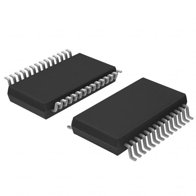
- Part No.:
- ASI4UE-G1-SR
- Manufacturer:
- Renesas
- Category:
- Specialized
- Package:
- 28-SSOP (0.209", 5.30mm Width)
- Datasheet:
-
 ASI4UE-G1-SR.pdf
- Description:
- IC INTERFACE SPECIALIZED 28SSOP
- Quantity:
- Payment:

- Shipping:

Inventory:8,770
Please send an inquiry. Send us your inquiry, and we will respond immediately.
Product details
Overview
ASI4UE-G1-SR from Integrated Device Technology is a universal AS-i interface IC compliant with AS-Interface Complete Specification V3.0, functioning as physical-layer transceiver and protocol handler in master/slave nodes. It delivers 55 mA current drive via on-chip electronic inductor, supports 8/16 MHz crystal auto-detection, operates from –25 °C to +85 °C, and integrates EEPROM for configuration storage - deployed in industrial sensor/actuator networks using two-wire AS-i bus.
For engineers reviewing the ASI4UE-G1-SR datasheet, ASI4UE-G1-SR pinout, ASI4UE-G1-SR application, or ASI4UE-G1-SR equivalent, this page provides verified technical context, validated pin functions, confirmed safety-mode behavior, real-world AS-i slave/master implementation constraints, and direct alternatives with documented functional trade-offs.
Technical Context
The ASI4UE-G1-SR implements dual-channel AS-i communication: primary Manchester-II encoded data channel (ASI+ / ASI−) and secondary IRD addressing channel for wireless setup. Its internal oscillator supports automatic 8/16 MHz crystal detection, and its digital I/O stage includes configurable input filters, bit-selective inversion, and synchronous data I/O mode for extended address profiles.
Thermal protection triggers shutdown at ≥150 °C; overload protection monitors UOUT/U5R outputs. The IC's safety mode disables input filtering and synchronous I/O to guarantee ≤40 ms fault reaction time - matching legacy A²SI timing - while standard mode enables enhanced preprocessing at the cost of added latency.
Key Specifications
| Parameter | Value and Actual Design Meaning |
|---|---|
| AS-i Compliance | Fully compliant with AS-Interface Complete Specification V3.0 - ensures interoperability with certified masters, slaves, and safety devices. |
| Operating Temperature | –25 °C to +85 °C - suitable for standard industrial control cabinets without forced cooling. |
| Package | SSOP28 RoHS-compliant - surface-mount footprint compatible with automated assembly and high-density PCB layouts. |
| Current Drive | 55 mA on-chip electronic inductor - eliminates need for external coil in basic AS-i bus power delivery. |
| Clock Support | Auto-detects 8 MHz or 16 MHz crystal - simplifies BOM management across frequency variants without firmware change. |
| Safety Mode Latency | Guaranteed ≤40 ms fault reaction time - matches A²SI timing when Safety Mode is enabled and input filters disabled. |
| EEPROM Storage | Internal non-volatile memory stores ID code, profile settings, and LED configuration - programmable via handheld or stationary programmer. |
Pinout & Package
ASI4UE-G1-SR uses a 28-pin SSOP package (5.6 mm × 10.2 mm, 0.65 mm pitch), optimized for industrial PCB space constraints and thermal dissipation in unshielded environments.
| Pin/Terminal | Circuit Role | Design Meaning |
|---|---|---|
| ASIP / ASIN | AS-i Bus Transceiver Inputs | Differential Manchester-II signal inputs - connect directly to two-wire AS-i cable; floating receiver enables symmetrical high-power operation. |
| UIN / UOUT / U5R | Power Supply Interface | UIN accepts 24 V AS-i bus voltage; UOUT supplies regulated 5 V to external logic; U5R provides 5 V reference for internal inductor driver. |
| DI[3:0] / DO[3:0] | Configurable Digital I/O | Four bidirectional data lines supporting 4I/4O processing in Extended Address Mode (Profile 7.A.x.E); direction controlled by DSR and PST. |
| IRD | Addressing Channel Input | AC or CMOS input for IR-based wireless addressing - enables setup without physical connection during commissioning. |
| P[3:0] / PST | Parameter Port | Serial interface for EEPROM programming and status readback; PST synchronizes parameter transfers and controls operational mode transitions. |
| FID | Fault Indication Input | Active-low input signaling power failure or thermal overload - triggers immediate bus error response in master/monitor modes. |
| LED1 / LED2 | Status Output Drivers | Configurable open-drain outputs supporting all V3.0 status indication modes (e.g., green/yellow flashing per device state). |
| OSC1 / OSC2 | Crystal Oscillator Terminals | Supports 8 MHz or 16 MHz fundamental-mode crystals - auto-detected at power-up; no external capacitors required for basic operation. |
Key Features
| Feature | Design Value |
|---|---|
| Universal node support | Configurable as master, slave, repeater, or bus monitor - single IC reduces BOM complexity across AS-i system roles. |
| Floating transmitter/receiver | Enables highly symmetrical high-power AS-i bus operation - critical for long-cable deployments with minimal signal distortion. |
| On-chip electronic inductor | Eliminates external coil component - reduces board area, assembly cost, and EMI susceptibility in compact modules. |
| V3.0-compliant LED status | Two dedicated LED drivers implement full AS-Interface status semantics (e.g., "addressed", "error", "safe") without MCU intervention. |
| Configurable input filtering | Adjustable time constants (100 µs to 10 ms) suppress contact bounce and EMI on DI[3:0] - improves reliability in noisy factory environments. |
| Safety Mode enforcement | Hardware-enforced disable of input filters and synchronous I/O - guarantees deterministic ≤40 ms fault reaction for certified safety applications. |
Applications
| AS-i Slave Module | AS-i Master Module |
|---|---|
|
Use Scenario: Connecting proximity sensors and solenoid valves in packaging machinery with minimal wiring. IC Role / Device Role / Timing Role: Physical layer interface handling AS-i bus power/data over two wires; manages address assignment and cyclic I/O exchange. Use Value: Reduces cabling cost by 70% vs. discrete I/O wiring; enables hot-plug device replacement without network interruption. |
Use Scenario: Central controller in automotive paint shop conveying AS-i commands to 32+ slave stations. IC Role / Device Role / Timing Role: Master node generating Manchester-II frames, managing timing cycles (≤5 µs jitter), and monitoring bus health. Use Value: Supports up to 62 slaves per segment; built-in watchdog ensures <100 ms recovery from bus faults. |
| AS-i Safety Module | AS-i Repeater |
|
Use Scenario: Emergency stop circuit in CNC machine tool requiring SIL 2 compliance. IC Role / Device Role / Timing Role: Safety-mode transceiver enforcing ≤40 ms fault reaction; validates safety code sequences (1110 pattern) before actuation. Use Value: Enables certified safety functionality without external timing supervision; maintains compatibility with legacy A²SI-based systems. |
Use Scenario: Extending AS-i bus length beyond 100 m in warehouse conveyor system. IC Role / Device Role / Timing Role: Signal regenerator restoring Manchester-II waveform integrity; isolates bus segments electrically and temporally. Use Value: Doubles effective bus length; prevents ground loop interference between zones while preserving cycle timing. |
Equivalent & Alternatives
The following parts are listed as comparable options for similar AS-i interface applications.
| Alternative Part | Technical Difference | Application Difference | Selection Advice |
|---|---|---|---|
| ASI4UE-G1-MR | Identical silicon, preconfigured for master mode via factory EEPROM setting - no runtime mode switching required. | Optimized for fixed-role master boards; lacks flexibility for field-reconfigurable slave/master use cases. | Select ASI4UE-G1-MR only if master-only function is guaranteed and EEPROM reprogramming is not needed post-deployment. |
| A²SI-28 | Legacy IDT AS-i IC; no on-chip inductor, no input filtering, no IRD channel, no Safety Mode - requires external coil and simpler EEPROM structure. | Compatible with older AS-i V2.1 designs; cannot support V3.0 features like extended addressing or safety certification upgrades. | Choose A²SI-28 only for cost-sensitive brownfield replacements where V3.0 features are unused and thermal margin is sufficient. |
Compared with ASI4UE-G1-SR, ASI4UE-G1-MR offers simplified master deployment but forfeits runtime configurability, while A²SI-28 provides proven reliability in legacy systems but lacks V3.0 compliance, safety mode, and integrated power delivery - making ASI4UE-G1-SR the only choice for new V3.0-certified or safety-enabled designs.
Availability
ASI4UE-G1-SR is available at Aetrix Electronics and suitable for AS-i slave modules, master controllers, safety-certified actuators, and repeater units requiring stable component supply across industrial automation, packaging equipment, and material handling systems.
Supply support for ASI4UE-G1-SR includes scheduled delivery planning, volume procurement assistance, BOM continuity management, traceable sourcing, and lifecycle availability coordination for OEM customers, industrial embedded developers, connected-device designers, and electronics production programs.
Manufacturer
Integrated Device Technology (IDT), now part of Renesas Electronics, is a semiconductor company specializing in timing, interface, and RF solutions for industrial and communications infrastructure.
The ASI4U family was designed specifically to replace legacy A²SI ICs in AS-i networks while adding V3.0 compliance, safety-mode determinism, and integrated power delivery - targeting next-generation industrial fieldbus modules.
FAQ
What is the operating temperature range for ASI4UE-G1-SR?
The ASI4UE-G1-SR operates from –25 °C to +85 °C, validated per datasheet Table 2.2. This range supports standard industrial cabinet environments without active cooling. It is distinct from the ASI4UE-E variant (–25 °C to +105 °C) and ASI4UE-F (–40 °C to +85 °C), both sharing the same SSOP28 package but differing in thermal qualification. ASI4UE-G1-SR must not be substituted into high-ambient designs without thermal derating analysis.
Does ASI4UE-G1-SR support AS-i Safety Mode, and how is it activated?
Yes, ASI4UE-G1-SR supports AS-i Safety Mode to guarantee ≤40 ms fault reaction time. Activation requires EEPROM configuration to disable input filters and synchronous data I/O - detailed in Section 3.3.10 and Section 4.7.6 of the datasheet. The safety code table in the host microcontroller must also be updated to accept only sequences containing "1110". Safety Mode is mandatory when replacing A²SI in certified safety modules.
What crystal frequencies does ASI4UE-G1-SR support, and is external tuning required?
ASI4UE-G1-SR supports 8 MHz and 16 MHz fundamental-mode crystals with automatic frequency detection at power-up. No external load capacitors are required for basic operation, though datasheet Table 4.22 specifies optional 12 pF caps for improved stability. The IC ignores harmonics or non-fundamental crystals; using unsupported frequencies results in oscillator failure and initialization halt.
How does the on-chip electronic inductor in ASI4UE-G1-SR compare to external coil solutions?
The ASI4UE-G1-SR integrates an electronic inductor delivering 55 mA drive capability, eliminating the need for external coil components in standard AS-i bus implementations. This reduces PCB area by ~25 mm², removes coil-related EMI concerns, and improves thermal coupling to the IC die. External coils remain necessary only for high-current (>55 mA) or ultra-long-cable (>300 m) applications per datasheet Section 4.18.1.
Is ASI4UE-G1-SR pin-compatible with the legacy A²SI IC?
Yes, ASI4UE-G1-SR is function and pin compatible with the A²SI IC per datasheet Section 1.1 and Figure 6.1. Identical SSOP28 pinout allows drop-in replacement in existing layouts. However, safety-critical A²SI-based modules must not be repaired with ASI4UE-G1-SR unless fully requalified - due to differences in data input routing and potential 40 ms latency increase in Standard Mode.
ASI4UE-G1-SR Specifications
- Product attributes
- Attribute value
- Manufacturer:
- Renesas
- Series:
- -
- Package/Case:
- 28-SSOP (0.209", 5.30mm Width)
- Packaging:
- Tape & Reel (TR)
- Product Status:
- Active
- Applications:
- Actuator Sensor Interface
- Interface:
- AS-i
- Voltage - Supply:
- 16V ~ 33.1V
- Supplier Device Package:
- 28-SSOP
- Grade:
- -
- Qualification:
- -
- Mounting Type:
- Surface Mount
ASI4UE-G1-SR FAQ
1.How can I place an order for ASI4UE-G1-SR through Aetrix?
Please submit a Request for Quotation (RFQ) for ASI4UE-G1-SR on Aetrix. Our sales agent will provide a competitive quotation and guide you through the order confirmation once you accept the terms.
2.Are the price and stock information for ASI4UE-G1-SR reliable?
The price and inventory of ASI4UE-G1-SR are updated periodically and may fluctuate due to market conditions. Stock and pricing data are typically refreshed every 24 hours. Quotation validity for ASI4UE-G1-SR is usually 5 days.
3.What payment methods are accepted for ASI4UE-G1-SR?
We accept Wire Transfer, PayPal, Credit Card, Western Union, MoneyGram, and Escrow for ASI4UE-G1-SR transactions.
Note: Certain payment methods may incur a processing fee.
4.How is shipping managed for ASI4UE-G1-SR?
ASI4UE-G1-SR orders can be shipped via leading logistics carriers, including DHL, UPS, FedEx, TNT, or Registered Mail.
Once your ASI4UE-G1-SR order is processed, you will receive an email with the shipment details and tracking number.
Note: Tracking information may take up to 24 hours to appear. Express delivery typically takes 3–5 business days.
5.How can I obtain technical support or documentation for ASI4UE-G1-SR?
For technical support, including ASI4UE-G1-SR datasheets, pinout diagrams, or application guidance, please contact our engineering support team. They can provide detailed documentation and assistance for your ASI4UE-G1-SR requirements.
6.How does Aetrix verify that ASI4UE-G1-SR is sourced from the original manufacturer or authorized distributors?
All ASI4UE-G1-SR products on Aetrix are procured from qualified distributors and authorized channels. Our dedicated quality assurance team conducts strict verification, including traceability checks and, if necessary, third-party testing. This ensures that ASI4UE-G1-SR meets industry standards.
7.What is the process for return or replacement of ASI4UE-G1-SR?
All ASI4UE-G1-SR units undergo pre-shipment inspection (PSI). If there is an issue with ASI4UE-G1-SR, returns or replacements are accepted under the following conditions:
1.Quantity discrepancies, incorrect items, or visible external defects (such as breakage or corrosion), acknowledged by Aetrix.
2.The issue is reported within 90 days of delivery.
3.The ASI4UE-G1-SR part is unused and in its original packaging.
Return procedure for ASI4UE-G1-SR:
1.Submit a request within 90 days.
2.Obtain a Return Material Authorization (RMA) from Aetrix.
ASI4UE-G1-SR Tags

-
NVT4857UKAZ
NXP Semiconductors

-
TCA8418RTWR
Texas Instruments

-
PCA9546APWR
Texas Instruments

-
MD0100N8-G
Microchip Technology

-
PCA9548APW,118
NXP Semiconductors

-
PCA9540BDP,118
NXP Semiconductors

-
PCA9548APWR
Texas Instruments

-
PCA9546APW,118
NXP Semiconductors

-
PTN3360DBS,518
NXP Semiconductors

-
PCA9546ABS,118
NXP Semiconductors

-
PCA9518PWR
Texas Instruments

-
PCA9545APW,118
NXP Semiconductors
Tech Hub

TTL and CMOS logic families differ in thresholds, loading, output drive, power and timing. This engineering guide compares 74HC and 74HCT, calculates noise margins and checks 3.3 V/5 V compatibility.

A practical engineering guide to 3.3V and 5V logic compatibility, input thresholds, resistor dividers, translator ICs, MOSFET level shifting, I2C pull-ups, timing limits and power-sequencing risks.

The 74HC595 uses push-pull logic outputs, while the TPIC6B595 uses 50 V open-drain DMOS sinks for higher-power loads. This guide compares timing, current limits, 3.3 V interfacing, load wiring, thermal…

The 74HC595 converts serial data into eight stable parallel outputs. This guide covers pin functions, shift and storage timing, OE and MR behavior, drive-current limits, cascading, voltage compatibilit…

A technical comparison of level-sensitive latches and edge-triggered flip-flops, covering timing windows, setup and hold limits, master–slave operation, time borrowing, race-through, HDL inference and…

A D latch stores one bit while Enable controls when data can pass. This reference covers gate-level operation, truth tables, transparency, setup and hold timing, LE versus OE, common ICs and practical …

An SR latch stores one bit through cross-coupled feedback. This engineering reference covers NOR and NAND implementations, truth tables, forbidden-state recovery, gated operation, switch debouncing, fa…

Latch circuits retain one bit through feedback. This technical reference covers SR and D latches, truth tables, transparency, timing limits, latch-versus-flip-flop behavior, applications and common log…

An engineering guide to LED driver operation, constant-current and constant-voltage outputs, linear and switching topologies, dimming, IC selection, calculations, replacement compatibility, and fault c…

Operational amplifier guide covering op amp basics, feedback, ideal vs real op amps, common configurations, buffer circuits, offset, bias current, gain-bandwidth, slew rate, rail-to-rail limits and sel…


