
 My Inquiry
 My Account


Renesas AT25DF021A-MHN-Y
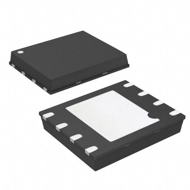
- Part No.:
- AT25DF021A-MHN-Y
- Manufacturer:
- Renesas
- Category:
- Memory
- Package:
- 8-UDFN Exposed Pad
- Datasheet:
-
 AT25DF021A-MHN-Y.pdf
- Description:
- IC FLASH 2MBIT SPI 104MHZ 8UDFN
- Quantity:
- Payment:

- Shipping:

Inventory:3,654
Please send an inquiry. Send us your inquiry, and we will respond immediately.
Product details
Overview
AT25DF021A-MHN-Y from Renesas Electronics is a 2-Mbit serial SPI Flash memory IC designed for code shadowing and embedded data storage in consumer electronics. It operates from 1.65 V to 3.6 V across –40°C to +85°C, supports Dual-I/O read mode at up to 104 MHz, delivers 6 ns clock-to-output timing, and features flexible erase granularity (256-byte page, 4/32/64-kByte blocks).
For engineers reviewing the AT25DF021A-MHN-Y datasheet, AT25DF021A-MHN-Y pinout, AT25DF021A-MHN-Y application, or AT25DF021A-MHN-Y equivalent, key selection criteria include SPI Mode 0/3 compatibility, hardware write protection via WP pin, OTP security register programmability, ultra-low deep power-down current (200 nA), and industrial-temperature-grade reliability.
Technical Context
The AT25DF021A-MHN-Y implements a standard SPI interface with dual I/O capability for accelerated read throughput, using SCK rising edge for input latching and falling edge for output clocking. Its memory architecture supports byte/page programming and four distinct erase granularities-page (256 B), 4-kB block, 32-kB block, and full chip-enabling efficient co-location of code and data without cross-contamination.
Protection is enforced via both software commands and hardware control through the WP pin, while sector locking states are managed by a dedicated status register. The device integrates a 128-byte OTP security register (64 bytes factory-unique, 64 bytes user-programmable) and supports active status interrupt reporting for asynchronous operation monitoring.
Key Specifications
| Parameter | Value and Actual Design Meaning |
|---|---|
| Memory Density | 2 Mbit (256 KByte) serial Flash array optimized for mixed code+data storage |
| Supply Voltage | 1.65 V–3.6 V single supply; enables direct interfacing with 1.8 V and 3.3 V microcontrollers |
| Max Clock Frequency | 104 MHz for Dual-Output Read; doubles effective data rate vs standard SPI reads |
| Read Latency | 6 ns clock-to-output (tV); critical for low-latency boot code execution |
| Erase Granularity | 256-byte page, 4-kB/32-kB/64-kB uniform blocks; minimizes wasted space in firmware updates |
| Power Consumption | 200 nA ultra-deep power-down current; extends battery life in always-on IoT endpoints |
| Endurance & Retention | 100,000 program/erase cycles and 20-year data retention at –40°C to +85°C |
Pinout & Package
AT25DF021A-MHN-Y is packaged in an 8-lead SOIC (150-mil) with standard JEDEC footprint and pinout. This package supports reflow soldering and is compatible with automated PCB assembly processes.
| Pin/Terminal | Circuit Role | Design Meaning |
|---|---|---|
| CS | Chip Select | Active-low enable signal; must transition high-to-low to initiate command sequence |
| SCK | Serial Clock | Master-generated clock; rising edge latches SI, falling edge clocks SO |
| SI (I/O0) | Serial Input / Dual-I/O Data Line 0 | Command/address/data input; becomes I/O0 during Dual-I/O read for parallel bit streaming |
| SO (I/O1) | Serial Output / Dual-I/O Data Line 1 | Data output line; remains active as I/O1 in Dual-I/O mode for simultaneous 2-bit reads |
| WP | Write Protect | Hardware lock control; low assertion disables write/erase commands to protected sectors |
| HOLD | Communication Hold | Pauses ongoing SPI transfer without deselecting device; requires CS low and SCK low to activate |
| VCC | Power Supply | 1.65–3.6 V input; powers all internal logic and memory array |
| GND | Ground Reference | System ground return path; required for stable voltage reference and noise immunity |
Key Features
| Feature | Design Value |
|---|---|
| Dual-I/O Read Mode | Delivers 2× data throughput vs standard SPI by clocking two bits per SCK falling edge |
| Flexible Erase Architecture | Enables independent update of firmware modules and configuration data without erasing adjacent regions |
| Hardware Write Protection | WP pin provides tamper-resistant sector locking independent of software state |
| OTP Security Register | 128-byte field with factory-unique 64-byte ID and user-programmable 64-byte space for secure keys or ESN |
| Ultra-Low Power Modes | 200 nA ultra-deep power-down current allows multi-year battery operation in sensor nodes |
Applications
| Smart Home Controller Firmware Storage | Industrial PLC Configuration Memory |
|---|---|
Use Scenario: Storing boot firmware and OTA update images in battery-powered smart thermostats and lighting hubs. IC Role / Device Role / Timing Role: Non-volatile code storage with fast Dual-I/O read enabling sub-100 ms application startup. Use Value: 6 ns tV latency and 104 MHz clock support reduce boot time; 256-byte page erase permits atomic firmware patching. | Use Scenario: Retaining calibrated sensor parameters and runtime configuration in DIN-rail mounted programmable logic controllers. IC Role / Device Role / Timing Role: Industrial-grade data logging and parameter backup memory with hardware write protection. Use Value: WP pin prevents accidental overwrites during field maintenance; 100K-cycle endurance ensures 10+ years of daily calibration saves. |
| Wearable Health Monitor Data Logger | Automotive Infotainment Boot Loader |
Use Scenario: Capturing heart-rate and motion sensor history in compact, coin-cell-powered wearables. IC Role / Device Role / Timing Role: Low-power persistent data buffer supporting intermittent writes and long-term retention. Use Value: 200 nA ultra-deep power-down current extends battery life beyond 12 months; 20-year data retention guarantees clinical record integrity. | Use Scenario: Hosting secure boot loader and cryptographic keys in automotive head units requiring ASIL-B alignment. IC Role / Device Role / Timing Role: Trusted execution environment (TEE) companion memory with OTP-based key storage. Use Value: Factory-programmed unique ID enables device authentication; OTP register prevents key extraction post-deployment. |
Equivalent & Alternatives
The following parts are listed as comparable options for similar serial Flash memory applications.
| Alternative Part | Technical Difference | Application Difference | Selection Advice |
|---|---|---|---|
| Winbond W25Q20EW | 2 Mbit density, 1.7–3.6 V supply, 133 MHz max clock, no OTP register, different status register map | Lacks factory-unique ID and user-programmable OTP; uses Quad-I/O instead of Dual-I/O | Select when higher clock speed and Quad-I/O bandwidth are prioritized over hardware-secured key storage |
| Micron MT25QL02G | 2 Gbit density (1000× larger), 1.7–2.0 V or 2.7–3.6 V dual supply options, Quad-SPI only, no 256-byte page erase | Not drop-in compatible due to density, voltage, and erase granularity mismatch; suited for high-capacity boot storage | Choose only for new designs requiring >1 Mbyte capacity and Quad-SPI ecosystem integration |
Compared with W25Q20EW and MT25QL02G, the AT25DF021A-MHN-Y uniquely balances fine-grained 256-byte erasure, integrated OTP security, and ultra-low 200 nA deep-sleep current-making it optimal for resource-constrained, security-aware embedded systems where code size and power budget are tightly constrained.
Availability
AT25DF021A-MHN-Y is available at Aetrix Electronics and suitable for smart home controllers, industrial PLCs, wearable health monitors, and automotive infotainment systems requiring stable component supply, long-term lifecycle support, and RoHS-compliant packaging.
Supply support for AT25DF021A-MHN-Y includes scheduled delivery planning, volume procurement assistance, BOM continuity management, traceable sourcing, and lifecycle availability coordination for OEM customers, industrial embedded developers, connected-device designers, and electronics production programs.
Manufacturer
Renesas Electronics is a global semiconductor leader delivering trusted microcontrollers, analog, power, and memory solutions for automotive, industrial, infrastructure, and IoT applications.
The AT25DF021A-MHN-Y belongs to Renesas' serial Flash memory product line, engineered specifically for cost-sensitive, low-power embedded systems needing reliable code storage, flexible data logging, and hardware-enforced security features.
FAQ
What is the operating temperature range supported by the AT25DF021A-MHN-Y?
The AT25DF021A-MHN-Y is rated for the full industrial temperature range of –40°C to +85°C. It also supports extended operation up to +125°C with derated endurance (20,000 cycles) and adjusted voltage limits (1.7–3.6 V). This makes the AT25DF021A-MHN-Y suitable for deployment in harsh environments such as factory automation and under-hood automotive modules where thermal stability is critical.
Does the AT25DF021A-MHN-Y support Quad-I/O or only Dual-I/O?
The AT25DF021A-MHN-Y supports SPI Modes 0 and 3 and Dual-I/O operation (using SI and SO as I/O0 and I/O1), but does not support Quad-I/O. Its Dual-I/O mode enables two bits per clock cycle during read operations, doubling throughput versus standard single-I/O SPI. Quad-I/O functionality is absent in the AT25DF021A-MHN-Y's command set and pin mapping per the official Renesas datasheet DS-AT25DF021A-042.
How is hardware write protection implemented on the AT25DF021A-MHN-Y?
Hardware write protection on the AT25DF021A-MHN-Y is controlled via the dedicated WP (Write Protect) pin, which is active-low. When asserted (pulled low), the WP pin locks protected sectors regardless of software command state-preventing accidental or malicious program/erase operations. The WP pin is internally pulled-high, so it may be left floating if unused, though Renesas recommends tying it to VCC for noise immunity. This complements software-based protection commands for defense-in-depth security.
What is the purpose and structure of the OTP security register in the AT25DF021A-MHN-Y?
The AT25DF021A-MHN-Y includes a 128-byte One-Time Programmable (OTP) security register: 64 bytes are factory-programmed with a unique identifier for device serialization, and 64 bytes are user-programmable for keys, certificates, or system-specific data. Once written, OTP locations cannot be erased or rewritten. This register supports secure boot, anti-counterfeiting, and electronic serial number (ESN) storage-critical for regulated or high-value embedded deployments where identity assurance is mandatory.
Can the AT25DF021A-MHN-Y be used in battery-powered applications with multi-year runtime requirements?
Yes-the AT25DF021A-MHN-Y is explicitly designed for ultra-low-power operation, drawing only 200 nA in Ultra Deep Power-Down mode (typical) and 4.5 µA in Deep Power-Down mode. Combined with 20-year data retention and 100,000 program/erase cycles, this enables decade-scale deployment in coin-cell or energy-harvesting systems like wireless sensors and medical wearables. Its 1.65 V minimum supply also supports direct integration with aging batteries down to ~1.7 V.
AT25DF021A-MHN-Y Specifications
- Product attributes
- Attribute value
- Manufacturer:
- Renesas
- Series:
- -
- Package/Case:
- 8-UDFN Exposed Pad
- Packaging:
- Tray
- Product Status:
- Active
- Programmable:
- Not Verified
- Memory Type:
- Non-Volatile
- Memory Format:
- FLASH
- Technology:
- FLASH
- Memory Size:
- 2Mbit
- Memory Organization:
- 256K x 8
- Memory Interface:
- SPI
- Clock Frequency:
- 104 MHz
- Write Cycle Time - Word, Page:
- 8µs, 2.5ms
- Access Time:
- -
- Voltage - Supply:
- 1.65V ~ 3.6V
- Operating Temperature:
- -40°C ~ 85°C (TC)
- Grade:
- -
- Qualification:
- -
- Mounting Type:
- Surface Mount
- Supplier Device Package:
- 8-UDFN (5x6)
AT25DF021A-MHN-Y FAQ
1.How can I place an order for AT25DF021A-MHN-Y through Aetrix?
Please submit a Request for Quotation (RFQ) for AT25DF021A-MHN-Y on Aetrix. Our sales agent will provide a competitive quotation and guide you through the order confirmation once you accept the terms.
2.Are the price and stock information for AT25DF021A-MHN-Y reliable?
The price and inventory of AT25DF021A-MHN-Y are updated periodically and may fluctuate due to market conditions. Stock and pricing data are typically refreshed every 24 hours. Quotation validity for AT25DF021A-MHN-Y is usually 5 days.
3.What payment methods are accepted for AT25DF021A-MHN-Y?
We accept Wire Transfer, PayPal, Credit Card, Western Union, MoneyGram, and Escrow for AT25DF021A-MHN-Y transactions.
Note: Certain payment methods may incur a processing fee.
4.How is shipping managed for AT25DF021A-MHN-Y?
AT25DF021A-MHN-Y orders can be shipped via leading logistics carriers, including DHL, UPS, FedEx, TNT, or Registered Mail.
Once your AT25DF021A-MHN-Y order is processed, you will receive an email with the shipment details and tracking number.
Note: Tracking information may take up to 24 hours to appear. Express delivery typically takes 3–5 business days.
5.How can I obtain technical support or documentation for AT25DF021A-MHN-Y?
For technical support, including AT25DF021A-MHN-Y datasheets, pinout diagrams, or application guidance, please contact our engineering support team. They can provide detailed documentation and assistance for your AT25DF021A-MHN-Y requirements.
6.How does Aetrix verify that AT25DF021A-MHN-Y is sourced from the original manufacturer or authorized distributors?
All AT25DF021A-MHN-Y products on Aetrix are procured from qualified distributors and authorized channels. Our dedicated quality assurance team conducts strict verification, including traceability checks and, if necessary, third-party testing. This ensures that AT25DF021A-MHN-Y meets industry standards.
7.What is the process for return or replacement of AT25DF021A-MHN-Y?
All AT25DF021A-MHN-Y units undergo pre-shipment inspection (PSI). If there is an issue with AT25DF021A-MHN-Y, returns or replacements are accepted under the following conditions:
1.Quantity discrepancies, incorrect items, or visible external defects (such as breakage or corrosion), acknowledged by Aetrix.
2.The issue is reported within 90 days of delivery.
3.The AT25DF021A-MHN-Y part is unused and in its original packaging.
Return procedure for AT25DF021A-MHN-Y:
1.Submit a request within 90 days.
2.Obtain a Return Material Authorization (RMA) from Aetrix.
AT25DF021A-MHN-Y Tags

-
M24C02-WMN6TP
STMicroelectronics

-
AT24C02C-XHM-T
Microchip Technology

-
AT21CS01-STUM10-T
Microchip Technology

-
AT24C02C-SSHM-T
Microchip Technology

-
24LC01BT-I/OT
Microchip Technology

-
M24C02-FMC6TG
STMicroelectronics
-
AT24CS02-SSHM-T
Microchip Technology

-
93LC46BT-I/OT
Microchip Technology
-
AT24C04C-SSHM-T
Microchip Technology

-
24LC01BT-I/SN
Microchip Technology
-
24AA02UIDT-I/OT
Microchip Technology

-
AT24C08C-STUM-T
Microchip Technology
Tech Hub

TTL and CMOS logic families differ in thresholds, loading, output drive, power and timing. This engineering guide compares 74HC and 74HCT, calculates noise margins and checks 3.3 V/5 V compatibility.

A practical engineering guide to 3.3V and 5V logic compatibility, input thresholds, resistor dividers, translator ICs, MOSFET level shifting, I2C pull-ups, timing limits and power-sequencing risks.

The 74HC595 uses push-pull logic outputs, while the TPIC6B595 uses 50 V open-drain DMOS sinks for higher-power loads. This guide compares timing, current limits, 3.3 V interfacing, load wiring, thermal…

The 74HC595 converts serial data into eight stable parallel outputs. This guide covers pin functions, shift and storage timing, OE and MR behavior, drive-current limits, cascading, voltage compatibilit…

A technical comparison of level-sensitive latches and edge-triggered flip-flops, covering timing windows, setup and hold limits, master–slave operation, time borrowing, race-through, HDL inference and…

A D latch stores one bit while Enable controls when data can pass. This reference covers gate-level operation, truth tables, transparency, setup and hold timing, LE versus OE, common ICs and practical …

An SR latch stores one bit through cross-coupled feedback. This engineering reference covers NOR and NAND implementations, truth tables, forbidden-state recovery, gated operation, switch debouncing, fa…

Latch circuits retain one bit through feedback. This technical reference covers SR and D latches, truth tables, transparency, timing limits, latch-versus-flip-flop behavior, applications and common log…

An engineering guide to LED driver operation, constant-current and constant-voltage outputs, linear and switching topologies, dimming, IC selection, calculations, replacement compatibility, and fault c…

Operational amplifier guide covering op amp basics, feedback, ideal vs real op amps, common configurations, buffer circuits, offset, bias current, gain-bandwidth, slew rate, rail-to-rail limits and sel…


