
 My Inquiry
 My Account


Microchip Technology AT49BV1614AT-70TI
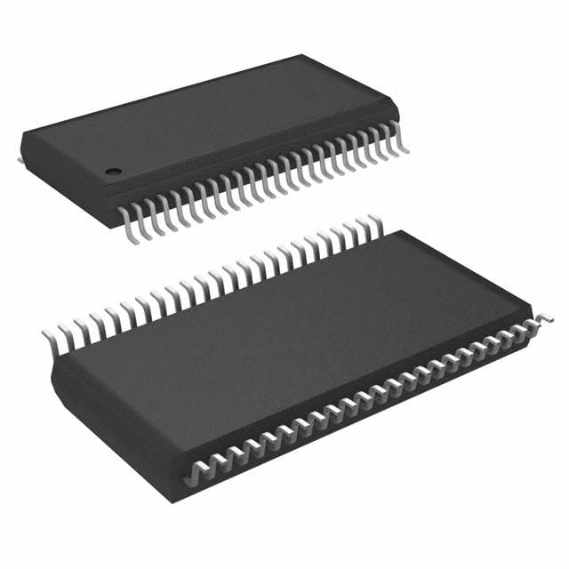
- Part No.:
- AT49BV1614AT-70TI
- Manufacturer:
- Microchip Technology
- Category:
- Memory
- Package:
- 48-TFSOP (0.724", 18.40mm Width)
- Datasheet:
-
 AT49BV1614AT-70TI.pdf
- Description:
- IC FLASH 16MBIT PARALLEL 48TSOP
- Quantity:
- Payment:

- Shipping:

Inventory:3,688
Please send an inquiry. Send us your inquiry, and we will respond immediately.
Product details
Overview
AT49BV1614AT-70TI from Microchip Technology (formerly Atmel) is a 16-megabit (1M × 16 / 2M × 8) 3.3V Flash memory IC with sector erase architecture, 70 ns access time, and dual-plane concurrent read/program-erase capability. It supports byte/word mode via BYTE pin, features erase suspend/resume, and operates in industrial temperature range (−40°C to +85°C) for embedded firmware storage in microcontroller-based systems.
For engineers reviewing the AT49BV1614AT-70TI datasheet, AT49BV1614AT-70TI pinout, AT49BV1614AT-70TI application, or AT49BV1614AT-70TI equivalent, key selection considerations include its 48-pin TSOP package, VPP-accelerated programming (5V/12V), 128-bit protection register, and sector lockdown for secure boot code retention.
Technical Context
The AT49BV1614AT-70TI implements a dual-plane Flash architecture: Plane A contains eight 4K-word and seven 32K-word sectors; Plane B contains twenty-four 32K-word sectors. This enables concurrent read from one plane while program/erase executes in the other - eliminating read latency during background updates.
Its command-set-driven operation uses six-byte sequences for chip/sector erase and lockdown, and supports hardware reset-initiated recovery from suspended erase or failed programming. The RDY/BUSY open-drain output, Data Polling (I/O7), and Toggle Bit (I/O6/I/O2) provide three independent methods to detect operation completion without polling overhead.
Key Specifications
| Parameter | Value and Actual Design Meaning |
|---|---|
| Memory Density | 16 Mbit (1,048,576 × 16 or 2,097,152 × 8) - supports firmware images up to 2 MB in byte mode or 1 MB in word mode |
| Access Time | 70 ns - enables direct execution from Flash (XIP) in timing-critical MCU boot paths |
| Supply Voltage | 2.65V–3.3V - compatible with modern low-voltage I/O domains and eliminates need for level shifters |
| Sector Architecture | 39 sectors (31 × 64 KB + 8 × 8 KB) - allows granular firmware partitioning (e.g., bootloader, app, config) |
| Program/Erase Speed | 20 µs/word; 300 ms/sector - balances update speed against write endurance and power burst requirements |
| Operating Temp | −40°C to +85°C - qualified for industrial control, automotive body electronics, and networking equipment |
| Package | 48-pin TSOP Type I (12 × 20 mm) - surface-mount compatible with standard reflow profiles and automated assembly |
Pinout & Package
AT49BV1614AT-70TI is packaged in a 48-pin Thin Small Outline Package (TSOP Type I), pin-compatible with industry-standard JEDEC MO-141AC. Pin 1 is marked by a notch or dot; pin numbering proceeds counterclockwise.
| Pin/Terminal | Circuit Role | Design Meaning |
|---|---|---|
| A0–A19 | Address Inputs | 20-bit address bus supporting full 1M-word addressing; A-1 function on I/O15 in byte mode |
| I/O0–I/O15 | Data I/O (x16) / I/O0–I/O7 + A-1 (x8) | Configurable data bus: BYTE=1 → x16; BYTE=0 → x8 with I/O15 repurposed as LSB address |
| CE, OE, WE | Chip Enable, Output Enable, Write Enable | Three-control read interface prevents bus contention; CE+OE low + WE high = read mode |
| RDY/BUSY | Open-drain status output | Active-low indicates ongoing program/erase; supports wired-OR of multiple devices on shared bus |
| VPP | Accelerated Program/Erase Supply | Accepts 5.0V ±0.5V or 12.0V ±0.5V to reduce tBP/tSEC; left unconnected for VCC-only operation |
| RESET | Hardware initialization input | Pulling low halts current operation and forces high-Z outputs; required to exit Single Pulse Program mode |
| BYTE | Bus width select | Logic high = 16-bit word mode; logic low = 8-bit byte mode with tri-stated I/O8–I/O14 |
| VCC, VCCQ, VSS | Core, I/O, and ground supplies | VCCQ decoupling enables mixed-voltage I/O (e.g., 3.3V core / 1.8V I/O) when regulated separately |
Key Features
| Feature | Design Value |
|---|---|
| Dual-plane concurrent operation | Enables real-time firmware updates: read active application from Plane B while erasing/programming Plane A |
| Erase suspend/resume | Interrupts sector erase to service urgent reads or writes elsewhere in same plane - critical for deterministic response in RTOS |
| 128-bit protection register | Factory-programmed 64-bit block A + user-writable/lockable block B - secures device identity and cryptographic keys |
| Sector lockdown | Per-sector write-protection activated via command; preserves bootloader integrity across field firmware upgrades |
| Hardware data protection | VCC sense, 10 ms power-on delay, noise filtering (<15 ns), and control-line inhibit prevent accidental writes |
Applications
| Industrial PLC Firmware Storage | Automotive Body Control Module |
|---|---|
Use Scenario: Storing ladder logic programs and configuration parameters in programmable logic controllers requiring field-upgradable nonvolatile memory. IC Role / Device Role / Timing Role: Primary firmware storage with sector-lockdown protecting boot loader and safety-critical routines. Use Value: Concurrent read/erase allows runtime updates without stopping machine control cycles; 70 ns access ensures deterministic scan times. | Use Scenario: Holding vehicle-specific calibration data, lighting control algorithms, and diagnostic firmware in body domain ECUs. IC Role / Device Role / Timing Role: Secure, temperature-hardened Flash for ASIL-B compliant subsystems with over-the-air update capability. Use Value: Erase suspend enables immediate response to door lock/unlock commands during background firmware validation; 128-bit register stores VIN-locked calibration keys. |
| Network Router Boot Memory | Medical Infusion Pump Firmware |
Use Scenario: Hosting bootloader, Linux kernel, and root filesystem in embedded network infrastructure equipment with remote management. IC Role / Device Role / Timing Role: Dual-plane Flash acting as XIP-capable boot device interfaced to ARM Cortex-A series processors. Use Value: 70 ns tACC supports zero-wait-state execution; VPP acceleration reduces firmware patch time during maintenance windows. | Use Scenario: Storing FDA-certified drug delivery algorithms, calibration tables, and audit logs in Class II medical devices. IC Role / Device Role / Timing Role: Tamper-resistant firmware repository with sector lockdown and protection register for regulatory traceability. Use Value: Hardware data protection prevents corruption during ESD events; industrial temp rating ensures reliability in hospital environments. |
Equivalent & Alternatives
The following parts are listed as comparable options for similar Flash memory applications.
| Alternative Part | Technical Difference | Application Difference | Selection Advice |
|---|---|---|---|
| SST39VF1601C-70-4C-EKE | Single-plane architecture; no erase suspend; 48-pin TSOP but different pinout (no VPP, no BYTE) | Lacks concurrent read/erase and sector lockdown - unsuitable for real-time update scenarios | Select only if system requires simpler command set and does not need dual-plane or secure boot features |
| MX29LV160ETTI-70G | Same density and 48-pin TSOP; supports CFI, but no VPP pin or 128-bit protection register | CFI compliance simplifies driver porting; lacks hardware-level sector lockdown and erase suspend | Prefer for legacy BIOS/UEFI platforms needing CFI support, but verify bootloader compatibility with missing security features |
Compared with SST39VF1601C-70-4C-EKE and MX29LV160ETTI-70G, the AT49BV1614AT-70TI uniquely delivers concurrent dual-plane operation, hardware-enforced sector lockdown, and a factory-programmed 128-bit identity register - making it the only option among the three qualified for secure, real-time firmware update architectures.
Availability
AT49BV1614AT-70TI is available at Aetrix Electronics and suitable for industrial automation, automotive electronics, and medical device manufacturing requiring stable component supply and long-term lifecycle assurance.
Supply support for AT49BV1614AT-70TI includes scheduled delivery planning, volume procurement assistance, BOM continuity management, traceable sourcing, and lifecycle availability coordination for OEM customers, industrial embedded developers, connected-device designers, and electronics production programs.
Manufacturer
Microchip Technology acquired Atmel in 2016 and maintains full support for the AT49BV/LV Flash family, including obsolescence mitigation and extended product change notifications.
The AT49BV/LV1614A(T) series was designed specifically for embedded systems requiring secure, in-system programmable Flash with real-time update capabilities - targeting applications where firmware integrity, field upgradeability, and deterministic timing are critical.
FAQ
What voltage levels are required for VPP to accelerate programming on the AT49BV1614AT-70TI?
The AT49BV1614AT-70TI requires VPP = 5.0V ± 0.5V or 12.0V ± 0.5V to enable accelerated program/erase operations. If VPP is unconnected or ≤ VCC, the device defaults to VCC-powered operation. Applying VPP within 0.3V of VCC (e.g., 3.0V VCC with 3.2V VPP) causes automatic fallback to VCC - ensuring robustness against marginal supply conditions. The AT49BV1614AT-70TI datasheet specifies these thresholds in the "VPP PIN" section.
How does the BYTE pin affect data bus configuration in the AT49BV1614AT-70TI?
When BYTE = high, the AT49BV1614AT-70TI operates in 16-bit word mode: I/O0–I/O15 are active data lines. When BYTE = low, it switches to 8-bit byte mode: only I/O0–I/O7 carry data, I/O8–I/O14 are tri-stated, and I/O15 functions as A-1 (LSB address). This dual-mode flexibility allows the same AT49BV1614AT-70TI to interface with both 8-bit and 16-bit microcontrollers without external glue logic.
Can the AT49BV1614AT-70TI perform read operations during an erase cycle?
Yes - the AT49BV1614AT-70TI's dual-plane architecture permits concurrent read from one memory plane while erasing or programming the other. For example, reading from Plane B is fully functional during a Plane A sector erase. If the target read sector resides in the same plane undergoing erase, the Erase Suspend command must first be issued to pause the erase and enable safe access - a capability confirmed in the "Erase Suspend/Resume" section of the AT49BV1614AT-70TI datasheet.
What is the purpose of the 128-bit protection register in the AT49BV1614AT-70TI?
The AT49BV1614AT-70TI's 128-bit protection register comprises two 64-bit blocks: Block A is factory-programmed with a unique, unchangeable identifier; Block B is user-programmable and lockable to store cryptographic keys or device-specific secrets. Once Block B is locked, its contents become read-only - preventing tampering while enabling secure boot verification. This feature is documented in the "128-BIT PROTECTION REGISTER" section of the AT49BV1614AT-70TI datasheet.
Does the AT49BV1614AT-70TI support hardware reset recovery from failed programming?
Yes - asserting RESET low during a program or erase cycle halts the operation and places all outputs in high-impedance state. Upon release, the AT49BV1614AT-70TI returns to read or standby mode, clearing internal state. This provides deterministic recovery from power glitches or watchdog timeouts. The AT49BV1614AT-70TI RESET functionality is detailed in the "RESET" subsection under "Device Operation", confirming its role in fault containment and system stability.
AT49BV1614AT-70TI Specifications
- Product attributes
- Attribute value
- Manufacturer:
- Microchip Technology
- Series:
- -
- Package/Case:
- 48-TFSOP (0.724", 18.40mm Width)
- Packaging:
- Tray
- Product Status:
- Obsolete
- Programmable:
- Not Verified
- Memory Type:
- Non-Volatile
- Memory Format:
- FLASH
- Technology:
- FLASH
- Memory Size:
- 16Mbit
- Memory Organization:
- 2M x 8, 1M x 16
- Memory Interface:
- Parallel
- Clock Frequency:
- -
- Write Cycle Time - Word, Page:
- 50µs
- Access Time:
- 70 ns
- Voltage - Supply:
- 2.65V ~ 3.3V
- Operating Temperature:
- -40°C ~ 85°C (TC)
- Grade:
- -
- Qualification:
- -
- Mounting Type:
- Surface Mount
- Supplier Device Package:
- 48-TSOP
AT49BV1614AT-70TI FAQ
1.How can I place an order for AT49BV1614AT-70TI through Aetrix?
Please submit a Request for Quotation (RFQ) for AT49BV1614AT-70TI on Aetrix. Our sales agent will provide a competitive quotation and guide you through the order confirmation once you accept the terms.
2.Are the price and stock information for AT49BV1614AT-70TI reliable?
The price and inventory of AT49BV1614AT-70TI are updated periodically and may fluctuate due to market conditions. Stock and pricing data are typically refreshed every 24 hours. Quotation validity for AT49BV1614AT-70TI is usually 5 days.
3.What payment methods are accepted for AT49BV1614AT-70TI?
We accept Wire Transfer, PayPal, Credit Card, Western Union, MoneyGram, and Escrow for AT49BV1614AT-70TI transactions.
Note: Certain payment methods may incur a processing fee.
4.How is shipping managed for AT49BV1614AT-70TI?
AT49BV1614AT-70TI orders can be shipped via leading logistics carriers, including DHL, UPS, FedEx, TNT, or Registered Mail.
Once your AT49BV1614AT-70TI order is processed, you will receive an email with the shipment details and tracking number.
Note: Tracking information may take up to 24 hours to appear. Express delivery typically takes 3–5 business days.
5.How can I obtain technical support or documentation for AT49BV1614AT-70TI?
For technical support, including AT49BV1614AT-70TI datasheets, pinout diagrams, or application guidance, please contact our engineering support team. They can provide detailed documentation and assistance for your AT49BV1614AT-70TI requirements.
6.How does Aetrix verify that AT49BV1614AT-70TI is sourced from the original manufacturer or authorized distributors?
All AT49BV1614AT-70TI products on Aetrix are procured from qualified distributors and authorized channels. Our dedicated quality assurance team conducts strict verification, including traceability checks and, if necessary, third-party testing. This ensures that AT49BV1614AT-70TI meets industry standards.
7.What is the process for return or replacement of AT49BV1614AT-70TI?
All AT49BV1614AT-70TI units undergo pre-shipment inspection (PSI). If there is an issue with AT49BV1614AT-70TI, returns or replacements are accepted under the following conditions:
1.Quantity discrepancies, incorrect items, or visible external defects (such as breakage or corrosion), acknowledged by Aetrix.
2.The issue is reported within 90 days of delivery.
3.The AT49BV1614AT-70TI part is unused and in its original packaging.
Return procedure for AT49BV1614AT-70TI:
1.Submit a request within 90 days.
2.Obtain a Return Material Authorization (RMA) from Aetrix.
AT49BV1614AT-70TI Tags

-
M24C02-WMN6TP
STMicroelectronics

-
AT24C02C-XHM-T
Microchip Technology

-
AT21CS01-STUM10-T
Microchip Technology

-
AT24C02C-SSHM-T
Microchip Technology

-
24LC01BT-I/OT
Microchip Technology

-
M24C02-FMC6TG
STMicroelectronics
-
AT24CS02-SSHM-T
Microchip Technology

-
93LC46BT-I/OT
Microchip Technology
-
AT24C04C-SSHM-T
Microchip Technology

-
24LC01BT-I/SN
Microchip Technology
-
24AA02UIDT-I/OT
Microchip Technology

-
AT24C08C-STUM-T
Microchip Technology
Tech Hub

TTL and CMOS logic families differ in thresholds, loading, output drive, power and timing. This engineering guide compares 74HC and 74HCT, calculates noise margins and checks 3.3 V/5 V compatibility.

A practical engineering guide to 3.3V and 5V logic compatibility, input thresholds, resistor dividers, translator ICs, MOSFET level shifting, I2C pull-ups, timing limits and power-sequencing risks.

The 74HC595 uses push-pull logic outputs, while the TPIC6B595 uses 50 V open-drain DMOS sinks for higher-power loads. This guide compares timing, current limits, 3.3 V interfacing, load wiring, thermal…

The 74HC595 converts serial data into eight stable parallel outputs. This guide covers pin functions, shift and storage timing, OE and MR behavior, drive-current limits, cascading, voltage compatibilit…

A technical comparison of level-sensitive latches and edge-triggered flip-flops, covering timing windows, setup and hold limits, master–slave operation, time borrowing, race-through, HDL inference and…

A D latch stores one bit while Enable controls when data can pass. This reference covers gate-level operation, truth tables, transparency, setup and hold timing, LE versus OE, common ICs and practical …

An SR latch stores one bit through cross-coupled feedback. This engineering reference covers NOR and NAND implementations, truth tables, forbidden-state recovery, gated operation, switch debouncing, fa…

Latch circuits retain one bit through feedback. This technical reference covers SR and D latches, truth tables, transparency, timing limits, latch-versus-flip-flop behavior, applications and common log…

An engineering guide to LED driver operation, constant-current and constant-voltage outputs, linear and switching topologies, dimming, IC selection, calculations, replacement compatibility, and fault c…

Operational amplifier guide covering op amp basics, feedback, ideal vs real op amps, common configurations, buffer circuits, offset, bias current, gain-bandwidth, slew rate, rail-to-rail limits and sel…


