
 My Inquiry
 My Account


Microchip Technology AT83C24B-TISUM
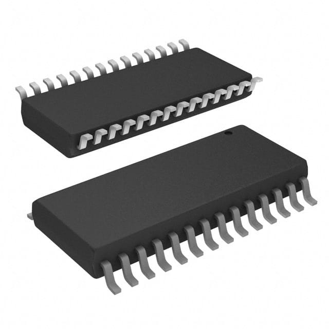
- Part No.:
- AT83C24B-TISUM
- Manufacturer:
- Microchip Technology
- Category:
- Specialized
- Package:
- 28-SOIC (0.295", 7.50mm Width)
- Datasheet:
-
 AT83C24B-TISUM.pdf
- Description:
- IC INTERFACE SPECIALIZED 28SO
- Quantity:
- Payment:

- Shipping:

Inventory:1,276
Please send an inquiry. Send us your inquiry, and we will respond immediately.
Product details
Overview
AT83C24B-TISUM from Microchip Technology is a smart card reader interface IC with integrated DC/DC converter, supporting ISO 7816, EMV2000, and GSM standards. It delivers programmable card supply voltages (5V ±5%, 3V ±0.2V, 1.8V ±0.14V), 8 kV+ ESD protection on card I/O pins, and operates from 4–48 MHz clock input. It is used in EFT/POS terminals and set-top boxes for secure, low-power smart card management.
For engineers reviewing the AT83C24B-TISUM datasheet, AT83C24B-TISUM pinout, AT83C24B-TISUM application, or AT83C24B-TISUM equivalent, key selection considerations include TWI-addressable multi-device configuration (up to 8), hardware- or software-controlled activation/deactivation sequences, CVCC voltage class compliance (Class A: 4.6–5.25 V), and SO28/QFN28 package compatibility with industrial temperature range (−40°C to +85°C).
Technical Context
The AT83C24B-TISUM implements a dual-mode power architecture: a high-efficiency (80–98%) step-up DC/DC converter for Class A/B card supply generation and an internal 3V regulator for digital core operation. Its TWI interface supports up to 400 kbit/s and enables full register-level control of card clock (CCLK), reset (CRST), I/O, C4/C8 contacts, and presence detection (CPRES).
It integrates dedicated hardware blocks including a 16-bit automatic reset transition (ART) timer for precise ATR timing compliance, programmable interrupt output (PRES/INT) with configurable IT_SEL mode, and transparent mode allowing direct microcontroller connection to CRST/CCLK via A1/RST and A2/CK pins - all synchronized to the 4–48 MHz master clock input.
Key Specifications
| Parameter | Value and Actual Design Meaning |
|---|---|
| Card Supply Voltage | Programmable: 5V ±5% (Class A), 3V ±0.2V (Class B), or 1.8V ±0.14V - enables single-chip support for all ISO 7816 voltage classes. |
| DC/DC Efficiency | 80–98% - minimizes thermal load and extends battery life in portable readers. |
| Input Clock Range | 4–48 MHz - supports wide host clock flexibility; ≥7 MHz required for step-up converter operation. |
| ESD Protection | 8 kV+ on CIO/CC4/CC8 pins (MIL-STD-883 Class 3) - ensures robustness against card insertion/removal transients. |
| Operating Temperature | −40°C to +85°C - qualified for industrial-grade EFT/POS and set-top box deployments. |
| Power-down Current | 30 µA typical (no card inserted) - enables ultra-low standby consumption in always-on terminals. |
| Supply Voltage Range | 3V to 5.5V on VCC - simplifies system power design with single-rail input. |
Pinout & Package
AT83C24B-TISUM is available in SO28 and QFN28 packages. Both variants share identical pin functions and electrical characteristics; pin numbering differs per package outline but signal mapping is consistent.
| Pin/Terminal | Circuit Role | Design Meaning |
|---|---|---|
| A2/CK | TWI address select / CCLK pass-through | Configures 7-bit slave address (with A1/RST and A0/3V); in transparent mode, directly routes host CLK to CCLK. |
| CRST | Smart card reset output | Drives card RST contact; controlled by CARDRST bit or A1/RST pin depending on CRST_SEL setting. |
| CIO | Smart card I/O bidirectional data | 8 kV+ ESD-protected interface to card I/O contact; level-shifted to CVCC voltage domain. |
| CVCC | Programmable card supply output | Delivers regulated 1.8V/3V/5V to smart card; requires external decoupling capacitor per datasheet layout guidelines. |
| PRES/INT | Open-drain interrupt/output | Signals card presence or error events (over-current, VCARDERR, ATR timeout); polarity and source configurable via IT_SEL bit. |
Key Features
| Feature | Design Value |
|---|---|
| ISO 7816-compliant activation sequence | Hardware- or software-triggered, with automatic deactivation on over-current, power fail, or card removal - eliminates firmware timing-critical handling. |
| Two-wire interface (TWI) | Up to 8 devices addressable on one bus using A2/A1/A0 pins; supports full register read/write for real-time card state monitoring and control. |
| Automatic Reset Transition (ART) | 16-bit hardware timer synchronizes CRST assertion to card clock cycles (tb ≥ 400 cycles), ensuring strict ISO 7816 ATR timing compliance without CPU intervention. |
| Integrated step-up DC/DC converter | Generates CVCC from 3–5.5V VCC input with 80–98% efficiency - removes need for external boost regulator and reduces BOM cost. |
| Card presence detection with filtering | CPRES pin supports programmable debounce (CDS[2:0]) and polarity inversion (CARDDET bit), enabling reliable detection across mechanical connector variations. |
Applications
| EFT/POS Terminal | Set-Top Box (STB) |
|---|---|
Use Scenario: Secure payment processing at retail point-of-sale using EMV-compliant chip cards. IC Role / Device Role / Timing Role: Smart card interface controller managing card power, clock, reset, and I/O signaling per ISO 7816-3 timing requirements. Use Value: Enables Class A (5V) and Class B (3V) card support in a single footprint; integrated DC/DC eliminates external boost circuitry, reducing PCB area and cost. | Use Scenario: Conditional access module in pay-TV STBs requiring NDS VideoGuard compatibility. IC Role / Device Role / Timing Role: Card interface with ART-timed reset and programmable voltage for secure decryption key exchange. Use Value: Meets NDS-specific minimum 18 MHz clock requirement and 3.3 µF CVCC capacitor constraint - validated for VideoGuard-certified designs. |
| Secure ID Reader | Government e-Passport Kiosk |
Use Scenario: Physical access control using ISO 7816-compliant ID cards in enterprise facilities. IC Role / Device Role / Timing Role: Host-side interface managing synchronous card activation, ATR parsing, and secure channel establishment. Use Value: 8 kV+ ESD protection on CIO/CC4/CC8 ensures reliability during frequent card swipes; low 30 µA shutdown current extends battery life in portable readers. | Use Scenario: Automated border control kiosks reading biometric e-passports compliant with ICAO Doc 9303. IC Role / Device Role / Timing Role: High-integrity card interface supporting dual-contact (C4/C8) and contactless coexistence modes. Use Value: Transparent mode allows direct connection to host MCU's ISO 7816 signals; programmable voltage and clock stop support legacy and next-gen passport chips. |
Equivalent & Alternatives
The following parts are listed as comparable options for similar smart card interface applications.
| Alternative Part | Technical Difference | Application Difference | Selection Advice |
|---|---|---|---|
| AT83C24NDS | Requires ≥18 MHz clock input; mandates 3.3 µF CVCC capacitor; Class A CVCC range tightened to 4.75–5.25 V. | Approved for NDS VideoGuard conditional access in STBs; not intended for general-purpose EFT/POS use. | Select AT83C24NDS only when NDS certification is mandatory; otherwise AT83C24B-TISUM offers broader clock and capacitor flexibility. |
| SLB9670 | TPM 2.0-compliant secure element with integrated crypto engine; no built-in DC/DC converter; requires external 3.3V supply. | Designed for trusted platform modules, not standalone smart card readers; lacks ISO 7816 physical layer drivers. | Choose SLB9670 for hardware-rooted security in PC/embedded hosts; AT83C24B-TISUM remains optimal for dedicated card reader front-ends. |
Compared with AT83C24NDS, AT83C24B-TISUM provides wider clock tolerance (4–48 MHz vs. 18–48 MHz) and relaxed CVCC capacitor requirements (up to 10 µF), making it more suitable for cost-sensitive, non-NDS-certified terminals. Versus SLB9670, AT83C24B-TISUM delivers full analog smart card interface functionality - including voltage regulation, ESD-hardened contacts, and ATR timing control - without requiring external power or signal conditioning.
Availability
AT83C24B-TISUM is available at Aetrix Electronics and suitable for EFT/POS terminals, set-top boxes, and secure ID readers requiring stable component supply across industrial temperature ranges and long product lifecycles.
Supply support for AT83C24B-TISUM includes scheduled delivery planning, volume procurement assistance, BOM continuity management, traceable sourcing, and lifecycle availability coordination for OEM customers, industrial embedded developers, connected-device designers, and electronics production programs.
Manufacturer
Microchip Technology is a U.S.-based semiconductor manufacturer specializing in microcontrollers, analog, and interface solutions for industrial, automotive, and consumer markets.
The AT83C24B-TISUM belongs to Microchip's Smart Card Interface Bus (SCIB) product line, designed specifically to simplify ISO 7816-compliant reader development with integrated power management, timing control, and robust physical layer protection.
FAQ
What is the minimum clock frequency required for AT83C24B-TISUM step-up converter operation?
The AT83C24B-TISUM requires a minimum 7 MHz clock input for proper operation of its internal step-up DC/DC converter. This is specified in the official datasheet (4234G–SCR–01/07, page 2). Clock frequencies below 7 MHz may prevent CVCC regulation and result in unstable card power delivery. The full operational range remains 4–48 MHz, but step-up functionality is only guaranteed above 7 MHz.
Does AT83C24B-TISUM support both 3V and 5V smart cards simultaneously?
No, AT83C24B-TISUM supports only one card voltage class per session: either 5V (Class A), 3V (Class B), or 1.8V - selected via VCARD[1:0] bits in CONFIG0 register. Switching between voltages requires full card deactivation first. The device does not provide concurrent dual-voltage outputs; CVCC is a single programmable rail. This behavior is confirmed in the "Activation Sequence" section (page 14) and electrical characteristics table.
How is card presence detected on AT83C24B-TISUM, and can the detection logic be inverted?
Card presence is detected via the CPRES pin, with polarity configurable using the CARDDET bit in CONFIG1 register. When CARDDET = 1, card presence is indicated by CPRES = 1 (open-collector pull-up to VCC); when CARDDET = 0, presence is CPRES = 0 (requires external pull-down). An internal pull-up can be enabled/disabled via the PULLUP bit. This dual-polarity support is documented in the "Card Presence Detection" section (page 10) and Figure 4.
Is AT83C24B-TISUM pin-compatible with AT83C24NDS?
Yes, AT83C24B-TISUM is pin-compatible with AT83C24NDS in both SO28 and QFN28 packages, sharing identical pinout, signal names, and electrical characteristics. However, functional differences exist: AT83C24NDS enforces stricter clock (≥18 MHz) and CVCC capacitor (3.3 µF mandatory) requirements. The shared pinout allows PCB reuse, but firmware and layout must comply with the specific variant's constraints.
What TWI address options are available for AT83C24B-TISUM, and how are they set?
AT83C24B-TISUM supports eight unique TWI slave addresses (0x40–0x4E for write, 0x41–0x4F for read), determined by the logic levels on A2/CK, A1/RST, and A0/3V pins at reset. Address sampling occurs on the 11th CLK rising edge after RESET assertion. This addressing scheme is defined in Table 2 (page 7) and enables up to eight devices on a single TWI bus without address conflict.
AT83C24B-TISUM Specifications
- Product attributes
- Attribute value
- Manufacturer:
- Microchip Technology
- Series:
- -
- Package/Case:
- 28-SOIC (0.295", 7.50mm Width)
- Packaging:
- Tube
- Product Status:
- Obsolete
- Applications:
- -
- Interface:
- 2-Wire
- Voltage - Supply:
- 3V ~ 5.5V
- Supplier Device Package:
- 28-SO
- Grade:
- -
- Qualification:
- -
- Mounting Type:
- Surface Mount
AT83C24B-TISUM FAQ
1.How can I place an order for AT83C24B-TISUM through Aetrix?
Please submit a Request for Quotation (RFQ) for AT83C24B-TISUM on Aetrix. Our sales agent will provide a competitive quotation and guide you through the order confirmation once you accept the terms.
2.Are the price and stock information for AT83C24B-TISUM reliable?
The price and inventory of AT83C24B-TISUM are updated periodically and may fluctuate due to market conditions. Stock and pricing data are typically refreshed every 24 hours. Quotation validity for AT83C24B-TISUM is usually 5 days.
3.What payment methods are accepted for AT83C24B-TISUM?
We accept Wire Transfer, PayPal, Credit Card, Western Union, MoneyGram, and Escrow for AT83C24B-TISUM transactions.
Note: Certain payment methods may incur a processing fee.
4.How is shipping managed for AT83C24B-TISUM?
AT83C24B-TISUM orders can be shipped via leading logistics carriers, including DHL, UPS, FedEx, TNT, or Registered Mail.
Once your AT83C24B-TISUM order is processed, you will receive an email with the shipment details and tracking number.
Note: Tracking information may take up to 24 hours to appear. Express delivery typically takes 3–5 business days.
5.How can I obtain technical support or documentation for AT83C24B-TISUM?
For technical support, including AT83C24B-TISUM datasheets, pinout diagrams, or application guidance, please contact our engineering support team. They can provide detailed documentation and assistance for your AT83C24B-TISUM requirements.
6.How does Aetrix verify that AT83C24B-TISUM is sourced from the original manufacturer or authorized distributors?
All AT83C24B-TISUM products on Aetrix are procured from qualified distributors and authorized channels. Our dedicated quality assurance team conducts strict verification, including traceability checks and, if necessary, third-party testing. This ensures that AT83C24B-TISUM meets industry standards.
7.What is the process for return or replacement of AT83C24B-TISUM?
All AT83C24B-TISUM units undergo pre-shipment inspection (PSI). If there is an issue with AT83C24B-TISUM, returns or replacements are accepted under the following conditions:
1.Quantity discrepancies, incorrect items, or visible external defects (such as breakage or corrosion), acknowledged by Aetrix.
2.The issue is reported within 90 days of delivery.
3.The AT83C24B-TISUM part is unused and in its original packaging.
Return procedure for AT83C24B-TISUM:
1.Submit a request within 90 days.
2.Obtain a Return Material Authorization (RMA) from Aetrix.
AT83C24B-TISUM Tags

-
NVT4857UKAZ
NXP Semiconductors

-
TCA8418RTWR
Texas Instruments

-
PCA9546APWR
Texas Instruments

-
MD0100N8-G
Microchip Technology

-
PCA9548APW,118
NXP Semiconductors

-
PCA9540BDP,118
NXP Semiconductors

-
PCA9548APWR
Texas Instruments

-
PCA9546APW,118
NXP Semiconductors

-
PTN3360DBS,518
NXP Semiconductors

-
PCA9546ABS,118
NXP Semiconductors

-
PCA9518PWR
Texas Instruments

-
PCA9545APW,118
NXP Semiconductors
Tech Hub

TTL and CMOS logic families differ in thresholds, loading, output drive, power and timing. This engineering guide compares 74HC and 74HCT, calculates noise margins and checks 3.3 V/5 V compatibility.

A practical engineering guide to 3.3V and 5V logic compatibility, input thresholds, resistor dividers, translator ICs, MOSFET level shifting, I2C pull-ups, timing limits and power-sequencing risks.

The 74HC595 uses push-pull logic outputs, while the TPIC6B595 uses 50 V open-drain DMOS sinks for higher-power loads. This guide compares timing, current limits, 3.3 V interfacing, load wiring, thermal…

The 74HC595 converts serial data into eight stable parallel outputs. This guide covers pin functions, shift and storage timing, OE and MR behavior, drive-current limits, cascading, voltage compatibilit…

A technical comparison of level-sensitive latches and edge-triggered flip-flops, covering timing windows, setup and hold limits, master–slave operation, time borrowing, race-through, HDL inference and…

A D latch stores one bit while Enable controls when data can pass. This reference covers gate-level operation, truth tables, transparency, setup and hold timing, LE versus OE, common ICs and practical …

An SR latch stores one bit through cross-coupled feedback. This engineering reference covers NOR and NAND implementations, truth tables, forbidden-state recovery, gated operation, switch debouncing, fa…

Latch circuits retain one bit through feedback. This technical reference covers SR and D latches, truth tables, transparency, timing limits, latch-versus-flip-flop behavior, applications and common log…

An engineering guide to LED driver operation, constant-current and constant-voltage outputs, linear and switching topologies, dimming, IC selection, calculations, replacement compatibility, and fault c…

Operational amplifier guide covering op amp basics, feedback, ideal vs real op amps, common configurations, buffer circuits, offset, bias current, gain-bandwidth, slew rate, rail-to-rail limits and sel…


