
 My Inquiry
 My Account


Microchip Technology AT83C26-RKTUL
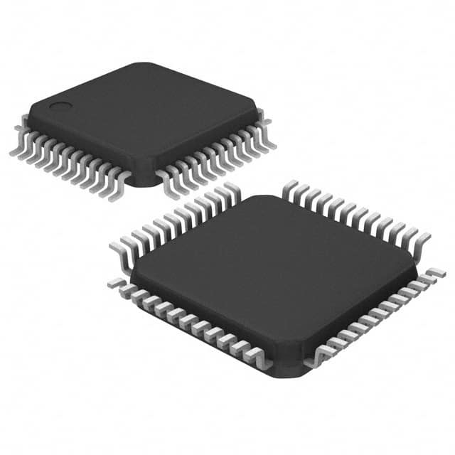
- Part No.:
- AT83C26-RKTUL
- Manufacturer:
- Microchip Technology
- Category:
- Specialized
- Package:
- 48-LQFP
- Datasheet:
-
 AT83C26-RKTUL.pdf
- Description:
- IC INTERFACE SPECIALIZED 48VQFP
- Quantity:
- Payment:

- Shipping:

Inventory:3,524
Please send an inquiry. Send us your inquiry, and we will respond immediately.
Product details
Overview
AT83C26-RKTUL from Microchip Technology is a smart card reader interface IC supporting up to five ISO 7816-compliant smart card interfaces with programmable voltage classes (1.8V/3V/5V), integrated DC/DC converters, TWI host interface at 400 kbit/s, and industrial temperature operation (–40°C to +85°C). It serves as the core power and protocol management IC in EFT/POS terminals and set-top box smart card readers.
For engineers reviewing the AT83C26-RKTUL datasheet, AT83C26-RKTUL pinout, AT83C26-RKTUL application, or AT83C26-RKTUL equivalent, this device delivers verified multi-card voltage regulation, card presence detection with filtering, automatic activation/deactivation sequencing, and dual DC/DC converter control - all critical for secure, low-power, multi-SIM/SAM embedded reader designs.
Technical Context
The AT83C26-RKTUL implements two independent DC/DC converters: DC/DCA powers SC1 (CVCC1) with pump/regulator mode selection via STEPREGA, while DC/DCB supplies CVCC2–CVCC5 through four LDOs. Its clock controller supports six outputs - five CCLKn signals (for smart cards 1–5) and one DCCLK - sourced from CLK, A2/CK, DCCLK, or CARDCKn bits.
Smart card I/O is managed via configurable bidirectional pins (CIO1–CIO5, CC41/CC81, etc.), with shared terminal arbitration between SC2 and SC3 (CRST3/CC82 and CIO3/CC42), controlled by SC2_CFG1's SC2_FULL bit. TWI address is set dynamically at reset via A1/RST and A2/CK pins, enabling up to four devices on one bus.
Key Specifications
| Parameter | Value and Actual Design Meaning |
|---|---|
| Smart Card Interfaces | 5 total: 1 dedicated SC1 + 4 shared SC2–SC5; SC2_FULL bit selects full SC2 (CC4/CC8) or SC3 interface |
| Supply Voltage Range | 3.0 V to 5.5 V - enables direct compatibility with common system rails without external regulators |
| Smart Card Voltage Classes | Class A (5V ±0.4V @ 60 mA), Class B (3V ±0.2V @ 60 mA), Class C (1.8V ±0.14V @ 40 mA) |
| Host Interface | Two-Wire Interface (TWI) at 400 kbit/s; programmable 7-bit slave address (0x42–0x4E write / 0x43–0x4F read) |
| DC/DC Converters | DC/DCA (for SC1) and DC/DCB (for SC2–SC5); each supports pump mode (inductor required) or regulator mode (VCC > output +0.3V) |
| ESD Protection | 4 kV HBM on smart card pins (CRST/CIO/CC4/CC8), 2 kV on other I/O - meets MIL-STD-883 Class 3 requirements |
| Operating Temperature | –40°C to +85°C - qualified for industrial-grade embedded reader applications |
| Quiescent Current | 30 µA typical in power-down mode (no smart card attached) - enables battery-backed or ultra-low-power standby |
Pinout & Package
AT83C26-RKTUL is available in QFN48 (7 mm × 7 mm, 0.5 mm pitch) and VQFP48 (7 mm × 7 mm, 0.5 mm pitch) packages. Both variants share identical pin functions and numbering.
| Pin/Terminal | Circuit Role | Design Meaning |
|---|---|---|
| CRST1, CRST2, CRST3/CC82, CRST4, CRST5 | Smart card reset outputs | Individually controllable RST signals; CRST3/CC82 and CIO3/CC42 are multiplexed based on SC2_FULL bit |
| CIO1–CIO5, CC41/CC42, CC81/CC82 | Smart card I/O and contact control | Bidirectional, pull-up configurable; transparent mode allows host-level signal routing via IO1/IO2/AUX1/AUX2 |
| CPRES1, CPRES2 | Card presence inputs | Detect insertion/removal; internal pull-up programmable (PULLUP1/PULLUP2 bits); filtering via CDS1[2:0]/CDS2[2:0] |
| SCL, SDA | TWI host interface | Open-drain, require external 4.7 kΩ pull-ups; support up to 4 devices via A1/RST and A2/CK address configuration |
| LIA, LIB | DC/DC converter inductor inputs | Connect to VCC via 10 µH inductor in pump mode; bypassed in regulator mode (STEPREGA/STEPREGB = 1) |
| CVCC1–CVCC5, CVCCB | Smart card supply outputs | CVCC1 driven by DC/DCA; CVCC2–CVCC5 regulated by LDOs from DC/DCB; dual CVCC1/CVCCB pins reduce noise |
| RESET | System reset I/O | Open-drain input/output; samples A1/RST and A2/CK at rising edge to set TWI address; triggers POR/PFD |
| INT | Interrupt output | Open-drain status flag; programmable internal pull-up (INT_PULLUP bit); asserts on card insert/extract, over-current, or voltage fault |
Key Features
| Feature | Design Value |
|---|---|
| Programmable smart card voltage per interface | Independent 1.8V/3V/5V selection per SC1–SC5 via VCARDn[1:0] registers - eliminates need for external voltage switches |
| Automatic activation/deactivation sequencing | Fully hardware-managed card power-up/down including ATR timing, clock stop (high/low), and deactivation on power-fail or over-current |
| Dual DC/DC architecture with LDO distribution | DC/DCA powers SC1; DC/DCB feeds four LDOs (LDO2–LDO5) for SC2–SC5 - enables scalable multi-card power with shared efficiency |
| Shared I/O arbitration with SC2/SC3 flexibility | CRST3/CC82 and CIO3/CC42 pins serve either SC3 or full SC2 (CC4/CC8) - software-configurable via SC2_CFG1 register |
| Configurable TWI address and interrupt behavior | A1/RST and A2/CK pins set 4 unique addresses (0x42–0x4E); INT output supports programmable pull-up and multiple event sources |
| Low-noise, low-ripple smart card supplies | <200 mV ripple on CVCC outputs - ensures stable card operation and compliance with ISO 7816 timing margins |
Applications
| EMV Payment Terminal | EFT/POS Reader Module |
|---|---|
|
Use Scenario: Secure contact-based payment processing in retail point-of-sale systems requiring EMV2000 and GIE-CB compliance. IC Role / Device Role / Timing Role: Manages dual smart card slots (primary card + SAM), provides isolated 3V/5V supplies, handles ATR negotiation, and executes secure deactivation on card removal. Use Value: Enables single-chip support for EMV-certified transactions with built-in short-circuit protection and 4 kV ESD - reducing BOM count and board space vs. discrete solutions. |
Use Scenario: Multi-interface financial transaction terminal integrating magnetic stripe, contactless, and contact smart card readers. IC Role / Device Role / Timing Role: Powers and controls up to five smart card interfaces (e.g., main card, backup card, three SAMs), synchronizes clock stops during low-power modes, and reports status via TWI. Use Value: Delivers deterministic activation timing and voltage regulation across all interfaces - meeting strict EMV timing windows and eliminating external DC/DC controllers. |
| Set-Top Box Conditional Access | Secure ID Authentication Terminal |
|
Use Scenario: Pay-TV set-top boxes using CI+ or DVB-CI modules with embedded smart card readers for content decryption. IC Role / Device Role / Timing Role: Supplies regulated 3V/5V to conditional access module (CAM) and SIM card; manages card presence detection and automatic power-down during standby. Use Value: Achieves <30 µA power-down current - extending battery life in portable STBs and ensuring reliable card hot-swap without system reset. |
Use Scenario: Government or enterprise identity verification kiosks requiring dual-PKI smart cards (e.g., PIV/CAC) and secure SAM co-processors. IC Role / Device Role / Timing Role: Controls two independent smart card interfaces with separate voltage classes (1.8V for PKI card, 3V for SAM), enforces card clock stop during authentication pauses. Use Value: Guarantees simultaneous, isolated power delivery and timing control - satisfying FIPS 201 and Common Criteria timing requirements for cryptographic operations. |
Equivalent & Alternatives
The following parts are listed as comparable options for similar smart card interface applications.
| Alternative Part | Technical Difference | Application Difference | Selection Advice |
|---|---|---|---|
| ST8024SW | Single smart card interface; no integrated DC/DC; requires external 3V/5V supplies; supports ISO 7816 only (no EMV2000/GSM extensions) | Limited to single-card, fixed-voltage readers; lacks multi-SAM support and automatic sequencing logic | Choose when cost sensitivity outweighs multi-card capability and power integration needs |
| MAX3232ESE+ | RS-232 transceiver only; no smart card interface logic, voltage regulation, or TWI host interface | Not functionally comparable - serves serial communication layer, not card reader subsystem | Not a functional alternative; consider only if replacing legacy RS-232 level-shifting in non-integrated designs |
Compared with ST8024SW and MAX3232ESE+, the AT83C26-RKTUL uniquely integrates five smart card interfaces, dual DC/DC converters, programmable voltage classes, and TWI-controlled sequencing - making it the only option capable of replacing discrete power, interface, and control circuitry in modern multi-SAM EFT/POS and conditional access systems.
Availability
AT83C26-RKTUL is available at Aetrix Electronics and suitable for EFT/POS terminals, set-top box conditional access modules, and secure ID authentication terminals requiring stable component supply, long-term lifecycle support, and industrial temperature resilience.
Supply support for AT83C26-RKTUL includes scheduled delivery planning, volume procurement assistance, BOM continuity management, traceable sourcing, and lifecycle availability coordination for OEM customers, industrial embedded developers, connected-device designers, and electronics production programs.
Manufacturer
Microchip Technology is a global semiconductor company specializing in microcontrollers, analog components, and security ICs, with broad expertise in embedded control and secure authentication solutions.
The AT83C26-RKTUL belongs to Microchip's Smart Card Interface IC product line, designed specifically to consolidate power management, protocol handling, and multi-card control into a single chip for EMV-compliant financial and identity verification systems.
FAQ
What smart card standards does the AT83C26-RKTUL support?
The AT83C26-RKTUL supports ISO/IEC 7816-3, EMV2000, GIE-CB, and GSM standards across all five smart card interfaces. It enables direct connection to synchronous cards (C4/C8 contacts), provides programmable voltage classes (1.8V/3V/5V), and implements full ATR timing control - ensuring interoperability with banking, telecom, and government-issued smart cards.
How does the AT83C26-RKTUL handle shared pins between SC2 and SC3?
The AT83C26-RKTUL uses CRST3/CC82 and CIO3/CC42 as multiplexed pins: when SC2_FULL = 1 in SC2_CFG1, they serve SC2's CC8 and CC4 functions; when SC2_FULL = 0, they become CRST3 and CIO3 for SC3. This hardware/software co-design allows flexible allocation without changing PCB layout - only firmware configuration determines interface assignment.
Can the AT83C26-RKTUL operate with only one smart card interface active?
Yes, the AT83C26-RKTUL supports partial interface activation. SC1 is fully independent; SC2–SC5 can be enabled individually via their respective configuration registers (e.g., SC2_CFG1, SC3_CFG2). Unused interfaces remain in low-power state, and their CVCC outputs default to 0 V - minimizing quiescent current and simplifying design for single-card applications like basic POS terminals.
What is the role of the BYPASS pin on the AT83C26-RKTUL?
The BYPASS pin on the AT83C26-RKTUL activates a low-power mode where internal bandgap references and regulators are switched off. To use it, SHUTDOWNA and SHUTDOWNB must first be set to disable both DC/DC converters. A high level on BYPASS then reduces total supply current to ~30 µA - ideal for battery-backed standby in portable smart card readers.
Does the AT83C26-RKTUL support hot-plug detection and automatic card deactivation?
Yes, the AT83C26-RKTUL provides hardware-accelerated hot-plug detection via CPRES1 and CPRES2 inputs with programmable filtering (CDS1[2:0]/CDS2[2:0]) and internal pull-up control. On card extraction, it initiates an automatic deactivation sequence - stopping CCLK, asserting CRST, and disabling CVCC - all without host intervention, ensuring safe, standards-compliant card removal.
AT83C26-RKTUL Specifications
- Product attributes
- Attribute value
- Manufacturer:
- Microchip Technology
- Series:
- -
- Package/Case:
- 48-LQFP
- Packaging:
- Tray
- Product Status:
- Obsolete
- Applications:
- -
- Interface:
- 2-Wire
- Voltage - Supply:
- 3V ~ 5.5V
- Supplier Device Package:
- 48-VQFP (7x7)
- Grade:
- -
- Qualification:
- -
- Mounting Type:
- Surface Mount
AT83C26-RKTUL FAQ
1.How can I place an order for AT83C26-RKTUL through Aetrix?
Please submit a Request for Quotation (RFQ) for AT83C26-RKTUL on Aetrix. Our sales agent will provide a competitive quotation and guide you through the order confirmation once you accept the terms.
2.Are the price and stock information for AT83C26-RKTUL reliable?
The price and inventory of AT83C26-RKTUL are updated periodically and may fluctuate due to market conditions. Stock and pricing data are typically refreshed every 24 hours. Quotation validity for AT83C26-RKTUL is usually 5 days.
3.What payment methods are accepted for AT83C26-RKTUL?
We accept Wire Transfer, PayPal, Credit Card, Western Union, MoneyGram, and Escrow for AT83C26-RKTUL transactions.
Note: Certain payment methods may incur a processing fee.
4.How is shipping managed for AT83C26-RKTUL?
AT83C26-RKTUL orders can be shipped via leading logistics carriers, including DHL, UPS, FedEx, TNT, or Registered Mail.
Once your AT83C26-RKTUL order is processed, you will receive an email with the shipment details and tracking number.
Note: Tracking information may take up to 24 hours to appear. Express delivery typically takes 3–5 business days.
5.How can I obtain technical support or documentation for AT83C26-RKTUL?
For technical support, including AT83C26-RKTUL datasheets, pinout diagrams, or application guidance, please contact our engineering support team. They can provide detailed documentation and assistance for your AT83C26-RKTUL requirements.
6.How does Aetrix verify that AT83C26-RKTUL is sourced from the original manufacturer or authorized distributors?
All AT83C26-RKTUL products on Aetrix are procured from qualified distributors and authorized channels. Our dedicated quality assurance team conducts strict verification, including traceability checks and, if necessary, third-party testing. This ensures that AT83C26-RKTUL meets industry standards.
7.What is the process for return or replacement of AT83C26-RKTUL?
All AT83C26-RKTUL units undergo pre-shipment inspection (PSI). If there is an issue with AT83C26-RKTUL, returns or replacements are accepted under the following conditions:
1.Quantity discrepancies, incorrect items, or visible external defects (such as breakage or corrosion), acknowledged by Aetrix.
2.The issue is reported within 90 days of delivery.
3.The AT83C26-RKTUL part is unused and in its original packaging.
Return procedure for AT83C26-RKTUL:
1.Submit a request within 90 days.
2.Obtain a Return Material Authorization (RMA) from Aetrix.
AT83C26-RKTUL Tags

-
NVT4857UKAZ
NXP Semiconductors

-
TCA8418RTWR
Texas Instruments

-
PCA9546APWR
Texas Instruments

-
MD0100N8-G
Microchip Technology

-
PCA9548APW,118
NXP Semiconductors

-
PCA9540BDP,118
NXP Semiconductors

-
PCA9548APWR
Texas Instruments

-
PCA9546APW,118
NXP Semiconductors

-
PTN3360DBS,518
NXP Semiconductors

-
PCA9546ABS,118
NXP Semiconductors

-
PCA9518PWR
Texas Instruments

-
PCA9545APW,118
NXP Semiconductors
Tech Hub

TTL and CMOS logic families differ in thresholds, loading, output drive, power and timing. This engineering guide compares 74HC and 74HCT, calculates noise margins and checks 3.3 V/5 V compatibility.

A practical engineering guide to 3.3V and 5V logic compatibility, input thresholds, resistor dividers, translator ICs, MOSFET level shifting, I2C pull-ups, timing limits and power-sequencing risks.

The 74HC595 uses push-pull logic outputs, while the TPIC6B595 uses 50 V open-drain DMOS sinks for higher-power loads. This guide compares timing, current limits, 3.3 V interfacing, load wiring, thermal…

The 74HC595 converts serial data into eight stable parallel outputs. This guide covers pin functions, shift and storage timing, OE and MR behavior, drive-current limits, cascading, voltage compatibilit…

A technical comparison of level-sensitive latches and edge-triggered flip-flops, covering timing windows, setup and hold limits, master–slave operation, time borrowing, race-through, HDL inference and…

A D latch stores one bit while Enable controls when data can pass. This reference covers gate-level operation, truth tables, transparency, setup and hold timing, LE versus OE, common ICs and practical …

An SR latch stores one bit through cross-coupled feedback. This engineering reference covers NOR and NAND implementations, truth tables, forbidden-state recovery, gated operation, switch debouncing, fa…

Latch circuits retain one bit through feedback. This technical reference covers SR and D latches, truth tables, transparency, timing limits, latch-versus-flip-flop behavior, applications and common log…

An engineering guide to LED driver operation, constant-current and constant-voltage outputs, linear and switching topologies, dimming, IC selection, calculations, replacement compatibility, and fault c…

Operational amplifier guide covering op amp basics, feedback, ideal vs real op amps, common configurations, buffer circuits, offset, bias current, gain-bandwidth, slew rate, rail-to-rail limits and sel…


