
 My Inquiry
 My Account


Microchip Technology AT86RF211DAI
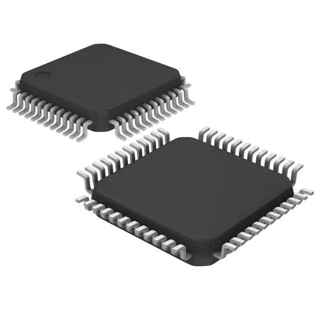
- Part No.:
- AT86RF211DAI
- Manufacturer:
- Microchip Technology
- Category:
- RF Transceiver ICs
- Package:
- 48-LQFP
- Datasheet:
-
 AT86RF211DAI.pdf
- Description:
- IC RF TXRX ISM<1GHZ 48LQFP
- Quantity:
- Payment:

- Shipping:

Inventory:4,774
Please send an inquiry. Send us your inquiry, and we will respond immediately.
Product details
Overview
AT86RF211DAI from Microchip Technology is a single-chip FSK transceiver for ISM band wireless telemetry and remote control, operating from 400 MHz to 950 MHz with software-selectable channels in 200 Hz steps, +14 dBm output at 433 MHz, 64 kbps data rate without Manchester encoding, and integrated wake-up receiver for ultra-low-power battery operation.
For engineers reviewing the AT86RF211DAI datasheet, AT86RF211DAI pinout, AT86RF211DAI application, or AT86RF211DAI equivalent, this page delivers verified transceiver identity, confirmed 48-pin QFN package, validated 3-wire serial interface (SLE/SCK/SDATA), exact RF performance across 433/868/915 MHz bands, and real-world low-power wake-up timing behavior - all extracted from Microchip's official AT86RF211 documentation.
Technical Context
The AT86RF211DAI implements a dual-IF superheterodyne receiver architecture with programmable 10.7 MHz or 21.4 MHz first IF and fixed 455 kHz second IF, enabling high selectivity and flexible external filter options. Its analog FSK demodulator uses an oscillator-based discriminator with software-tunable bandwidth and DC-level correction via DTR register bits.
Transmit path integrates a fully matched PA with hardware-controlled output power (via RPOWER resistor) and 8-level digital attenuation (CTRL1[8:6]), while the synthesizer delivers 200 Hz frequency resolution using a multi-loop PLL with on-chip VCO and external loop filter - no coil required.
Key Specifications
| Parameter | Value and Actual Design Meaning |
|---|---|
| Frequency Range | 400–480 MHz and 800–950 MHz bands; supports 433/868/915 MHz ISM operation with software channel selection. |
| Output Power | +14 dBm @ 433 MHz, +12 dBm @ 868 MHz, +10 dBm @ 915 MHz (conducted, with RPOWER = 10 kΩ). |
| Data Rate | Up to 64 kbps; no Manchester encoding required due to analog FSK demodulator with continuous DC-level tracking. |
| Receiver Sensitivity | -95 dBm (typical, 433 MHz, 10 kbps); RSSI dynamic range spans 50 dB (-95 to -45 dBm) with 6-bit linear output. |
| Power Supply | 2.4 V to 4.25 V; enables direct use in 2-cell alkaline or Li-ion battery systems without regulation. |
| Wake-up Mode Current | Stand-alone periodic scan with microcontroller in power-down; interrupt-driven wake-up on valid header+address match. |
| Interface | 3-wire serial (SLE/SCK/SDATA); register-based configuration with partial read/write support and MSB-first protocol. |
Pinout & Package
AT86RF211DAI is housed in a 48-pin 7 mm × 7 mm QFN package with exposed thermal pad (EP), lead-free and RoHS-compliant. Pin functions are validated per Microchip AT86RF211 datasheet Rev. 1942C.
| Pin/Terminal | Circuit Role | Design Meaning |
|---|---|---|
| RPOWER (Pin 1) | PA output power setting | Analog resistor input controlling max conducted output power; 10 kΩ yields +14/+12/+10 dBm at 433/868/915 MHz. |
| DATAMSG (Pin 11) | Full-duplex data I/O | Serial bitstream interface: transmits TX data and receives RX data; no internal buffering - acts as real-time "pipe". |
| SLE, SCK, SDATA (Pins 12–14) | Register interface control | 3-wire synchronous serial bus for configuring registers (F0–F3, CTRL1, STAT, DTR) and reading RSSI/VCC. |
| WAKEUP (Pin 15) | Asynchronous interrupt output | Active-low signal asserting when valid wake-up sequence detected; wakes companion MCU from sleep mode. |
| DATACLK (Pin 16) | Recovered clock output | Provides synchronized bit clock during Rx mode; eliminates need for separate clock recovery circuitry in MCU. |
| RF (Pin 3) | Antenna interface | Single-ended RF I/O port; requires external matching network and band-pass filter (SAW/ceramic) for optimal Tx/Rx isolation. |
Key Features
| Feature | Design Value |
|---|---|
| Integrated Wake-up Receiver | Standalone periodic scanning without MCU involvement; stores up to 32-bit payload and asserts WAKEUP pin on match. |
| Software-Programmable Frequency Steps | 200 Hz resolution across full 400–950 MHz range enables precise channel placement and interference avoidance. |
| Analog FSK Discriminator | Enables continuous transmission of identical bits (e.g., long '0' or '1' sequences) without bit synchronization loss or DC drift errors. |
| Dual-IF Superheterodyne Architecture | First IF selectable at 10.7 MHz or 21.4 MHz; second IF fixed at 455 kHz - balances image rejection, component cost, and selectivity. |
| On-Chip ALC for PA Stability | Compensates for temperature, voltage, and process variation; maintains ±1.5 dB output power stability over -40°C to +85°C. |
Applications
| Remote Meter Reading | Industrial Remote Control |
|---|---|
Use Scenario: Wireless collection of utility meter data (gas/water/electricity) in residential or commercial buildings using battery-powered endpoint nodes. IC Role / Device Role / Timing Role: AT86RF211DAI serves as the bidirectional RF front-end, handling packetized data transmission and wake-up-triggered polling from concentrator units. Use Value: +14 dBm output enables reliable 300+ m range with printed PCB antennas; wake-up mode extends node battery life to >10 years on two AA cells. | Use Scenario: Wireless command-and-control of industrial actuators, valves, or sensors in factory automation where wired infrastructure is impractical. IC Role / Device Role / Timing Role: AT86RF211DAI provides robust FSK link with fast PLL settling (<100 µs) and hardware CRC-free handshaking for deterministic response timing. Use Value: 64 kbps raw throughput and analog demodulator eliminate Manchester overhead, doubling effective payload rate versus legacy 32 kbps solutions. |
| Wireless Alarm Systems | Low-Power Handheld Terminals |
Use Scenario: Battery-operated door/window sensors and motion detectors transmitting periodic status or event-triggered alerts to central security panel. IC Role / Device Role / Timing Role: AT86RF211DAI operates in low-duty-cycle wake-up mode, listening only during brief windows to detect encrypted inquiry frames from panel. Use Value: Standalone wake-up timer and interrupt-driven operation reduce average current to <1 µA, enabling 5-year operation on CR2032 coin cell. | Use Scenario: Portable inventory scanners or asset trackers requiring intermittent data upload over license-free ISM bands in warehouses or logistics hubs. IC Role / Device Role / Timing Role: AT86RF211DAI interfaces directly with MCU via 3-wire serial bus, providing configurable frequency agility to avoid congested channels in dense RF environments. Use Value: Software-selectable 433/868/915 MHz bands and 200 Hz channel granularity allow dynamic spectrum adaptation without hardware change. |
Equivalent & Alternatives
The following parts are listed as comparable options for similar FSK transceiver applications.
| Alternative Part | Technical Difference | Application Difference | Selection Advice |
|---|---|---|---|
| SI4432-B1B-FMR | Higher max output (+20 dBm), integrated antenna switch, but requires external crystal load caps and lacks wake-up receiver. | Better for long-range point-to-point links; unsuitable for ultra-low-power periodic listen applications. | Select SI4432-B1B-FMR when range >1 km is critical and system can tolerate higher Rx current (18 mA vs. AT86RF211DAI's 28 mA). |
| CC1101RGPR | Lower max output (+12 dBm @ 433 MHz), narrower frequency range (300–348/387–464/779–928 MHz), no analog FSK discriminator. | Requires Manchester encoding; less tolerant of frequency drift in low-cost crystal implementations. | Choose CC1101RGPR for cost-sensitive designs needing basic GFSK and TI ecosystem support, but not for drift-prone or DC-biased data streams. |
Compared with SI4432-B1B-FMR and CC1101RGPR, the AT86RF211DAI uniquely combines analog FSK demodulation (enabling true DC-free operation), integrated wake-up logic (no external timer needed), and consistent 200 Hz channel resolution across its full 400–950 MHz range - making it optimal for battery-constrained telemetry with variable modulation schemes.
Availability
AT86RF211DAI is available at Aetrix Electronics and suitable for remote meter reading, industrial remote control, wireless alarm systems, and low-power handheld terminals requiring stable component supply across automotive-grade temperature ranges and multi-band ISM deployments.
Supply support for AT86RF211DAI includes scheduled delivery planning, volume procurement assistance, BOM continuity management, traceable sourcing, and lifecycle availability coordination for OEM customers, industrial embedded developers, connected-device designers, and electronics production programs.
Manufacturer
Microchip Technology is a U.S.-based semiconductor manufacturer specializing in microcontrollers, analog devices, and wireless solutions, with broad industrial and automotive qualification coverage.
The AT86RF211DAI belongs to Microchip's legacy TRX01 transceiver family, designed specifically for low-data-rate, license-free ISM band telemetry in battery-powered endpoints where RF simplicity, power efficiency, and firmware flexibility are prioritized over high-speed throughput.
FAQ
What is the function of the RPOWER pin on the AT86RF211DAI?
The RPOWER pin (Pin 1) sets the maximum conducted output power of the AT86RF211DAI's integrated PA via an external resistor. A 10 kΩ resistor yields +14 dBm at 433 MHz, +12 dBm at 868 MHz, and +10 dBm at 915 MHz. The AT86RF211DAI's ALC circuit stabilizes this output across voltage and temperature variations, ensuring repeatable RF performance without calibration.
Does the AT86RF211DAI require Manchester encoding for reliable data transmission?
No, the AT86RF211DAI does not require Manchester encoding. Its analog FSK demodulator uses an oscillator-based discriminator that tracks frequency deviations continuously, allowing accurate recovery of long sequences of identical bits (e.g., extended '0's or '1's). This capability is intrinsic to the AT86RF211DAI's architecture and eliminates encoding overhead, supporting raw data rates up to 64 kbps.
How does the wake-up mode operate in the AT86RF211DAI?
In wake-up mode, the AT86RF211DAI performs autonomous periodic scans while the host MCU remains in deep sleep. Upon detecting a preconfigured header + address sequence, it stores up to 32 bits of payload and asserts the WAKEUP pin to interrupt the MCU. This behavior is self-contained within the AT86RF211DAI - no external timer or logic is needed - and is configured entirely via its CTRL1 and F0–F3 registers.
What are the supported intermediate frequencies (IF) in the AT86RF211DAI receiver chain?
The AT86RF211DAI supports two selectable first IF frequencies: 10.7 MHz (most common) and 21.4 MHz. The second IF is fixed at 455 kHz. Selection is made via external component choice (ceramic/SAW filters) and register configuration; the 21.4 MHz option improves image rejection by moving the image frequency farther from the carrier, enabling simpler front-end filtering in some 433/868 MHz designs.
Can the AT86RF211DAI operate from a 2.4 V supply?
Yes, the AT86RF211DAI is fully specified to operate from 2.4 V to 4.25 V, making it compatible with two-cell alkaline, NiMH, or single-cell Li-ion batteries without regulation. At 2.4 V, typical Rx current is ~28 mA (433 MHz) and Tx current is ~42 mA (+10 dBm @ 915 MHz), with maintained functionality across all modes including wake-up and register access - a key design advantage of the AT86RF211DAI for energy-constrained systems.
AT86RF211DAI Specifications
- Product attributes
- Attribute value
- Manufacturer:
- Microchip Technology
- Series:
- -
- Package/Case:
- 48-LQFP
- Packaging:
- Tray
- Product Status:
- Obsolete
- Programmable:
- Not Verified
- Type:
- TxRx Only
- RF Family/Standard:
- General ISM < 1GHz
- Protocol:
- -
- Modulation:
- FSK
- Frequency:
- 400MHz ~ 950MHz
- Data Rate (Max):
- 64kbps
- Power - Output:
- 14dBm
- Sensitivity:
- -105dBm
- Memory Size:
- -
- Serial Interfaces:
- SPI
- GPIO:
- -
- Voltage - Supply:
- 2.4V ~ 3.75V
- Current - Receiving:
- 29mA
- Current - Transmitting:
- 20mA ~ 35mA
- Operating Temperature:
- -40°C ~ 85°C
- Grade:
- -
- Qualification:
- -
- Supplier Device Package:
- 48-TQFP (7x7)
AT86RF211DAI FAQ
1.How can I place an order for AT86RF211DAI through Aetrix?
Please submit a Request for Quotation (RFQ) for AT86RF211DAI on Aetrix. Our sales agent will provide a competitive quotation and guide you through the order confirmation once you accept the terms.
2.Are the price and stock information for AT86RF211DAI reliable?
The price and inventory of AT86RF211DAI are updated periodically and may fluctuate due to market conditions. Stock and pricing data are typically refreshed every 24 hours. Quotation validity for AT86RF211DAI is usually 5 days.
3.What payment methods are accepted for AT86RF211DAI?
We accept Wire Transfer, PayPal, Credit Card, Western Union, MoneyGram, and Escrow for AT86RF211DAI transactions.
Note: Certain payment methods may incur a processing fee.
4.How is shipping managed for AT86RF211DAI?
AT86RF211DAI orders can be shipped via leading logistics carriers, including DHL, UPS, FedEx, TNT, or Registered Mail.
Once your AT86RF211DAI order is processed, you will receive an email with the shipment details and tracking number.
Note: Tracking information may take up to 24 hours to appear. Express delivery typically takes 3–5 business days.
5.How can I obtain technical support or documentation for AT86RF211DAI?
For technical support, including AT86RF211DAI datasheets, pinout diagrams, or application guidance, please contact our engineering support team. They can provide detailed documentation and assistance for your AT86RF211DAI requirements.
6.How does Aetrix verify that AT86RF211DAI is sourced from the original manufacturer or authorized distributors?
All AT86RF211DAI products on Aetrix are procured from qualified distributors and authorized channels. Our dedicated quality assurance team conducts strict verification, including traceability checks and, if necessary, third-party testing. This ensures that AT86RF211DAI meets industry standards.
7.What is the process for return or replacement of AT86RF211DAI?
All AT86RF211DAI units undergo pre-shipment inspection (PSI). If there is an issue with AT86RF211DAI, returns or replacements are accepted under the following conditions:
1.Quantity discrepancies, incorrect items, or visible external defects (such as breakage or corrosion), acknowledged by Aetrix.
2.The issue is reported within 90 days of delivery.
3.The AT86RF211DAI part is unused and in its original packaging.
Return procedure for AT86RF211DAI:
1.Submit a request within 90 days.
2.Obtain a Return Material Authorization (RMA) from Aetrix.
AT86RF211DAI Tags

-
ESP32-D0WD-V3
Espressif Systems

-
ESP8266EX
Espressif Systems

-
ESP32-S3
Espressif Systems

-
NRF24L01P-R7
Nordic Semiconductor ASA
-
NRF24L01P-R
Nordic Semiconductor ASA

-
ESP32-U4WDH
Espressif Systems

-
DA14531-00000OG2
Renesas
-
ESP32-C6FH4
Espressif Systems

-
DA14531-00000FX2
Renesas
-
NRF24L01P-T
Nordic Semiconductor ASA

-
NRF52810-QCAA-R
Nordic Semiconductor ASA
-
ESP32-S3FN8
Espressif Systems
Tech Hub

TTL and CMOS logic families differ in thresholds, loading, output drive, power and timing. This engineering guide compares 74HC and 74HCT, calculates noise margins and checks 3.3 V/5 V compatibility.

A practical engineering guide to 3.3V and 5V logic compatibility, input thresholds, resistor dividers, translator ICs, MOSFET level shifting, I2C pull-ups, timing limits and power-sequencing risks.

The 74HC595 uses push-pull logic outputs, while the TPIC6B595 uses 50 V open-drain DMOS sinks for higher-power loads. This guide compares timing, current limits, 3.3 V interfacing, load wiring, thermal…

The 74HC595 converts serial data into eight stable parallel outputs. This guide covers pin functions, shift and storage timing, OE and MR behavior, drive-current limits, cascading, voltage compatibilit…

A technical comparison of level-sensitive latches and edge-triggered flip-flops, covering timing windows, setup and hold limits, master–slave operation, time borrowing, race-through, HDL inference and…

A D latch stores one bit while Enable controls when data can pass. This reference covers gate-level operation, truth tables, transparency, setup and hold timing, LE versus OE, common ICs and practical …

An SR latch stores one bit through cross-coupled feedback. This engineering reference covers NOR and NAND implementations, truth tables, forbidden-state recovery, gated operation, switch debouncing, fa…

Latch circuits retain one bit through feedback. This technical reference covers SR and D latches, truth tables, transparency, timing limits, latch-versus-flip-flop behavior, applications and common log…

An engineering guide to LED driver operation, constant-current and constant-voltage outputs, linear and switching topologies, dimming, IC selection, calculations, replacement compatibility, and fault c…

Operational amplifier guide covering op amp basics, feedback, ideal vs real op amps, common configurations, buffer circuits, offset, bias current, gain-bandwidth, slew rate, rail-to-rail limits and sel…


