
 My Inquiry
 My Account


Microchip Technology ATA5429-PLQW
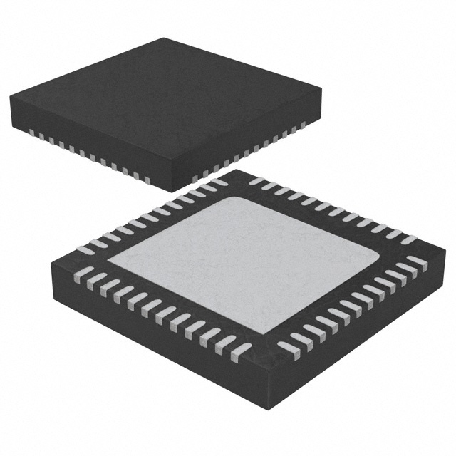
- Part No.:
- ATA5429-PLQW
- Manufacturer:
- Microchip Technology
- Category:
- RF Transceiver ICs
- Package:
- 48-VFQFN Exposed Pad
- Datasheet:
-
 ATA5429-PLQW.pdf
- Description:
- IC RF TXRX ISM<1GHZ 48VQFN
- Quantity:
- Payment:

- Shipping:

Inventory:1,362
Please send an inquiry. Send us your inquiry, and we will respond immediately.
Product details
Overview
ATA5429-PLQW from Microchip Technology is a highly integrated UHF ASK/FSK multi-channel half-duplex transceiver operating in the 912.5–917.5 MHz band, featuring ±2.5 MHz programmable tuning range, –103.5 dBm FSK sensitivity at 20 kBaud, –109.5 dBm ASK sensitivity at 2.4 kBaud, and 0–10 dBm adjustable output power. It integrates RX/TX switch, fractional-N synthesizer, low-IF signal processing (226 kHz IF), RSSI, SPI interface (≤500 kbit/s), and 5 push-button inputs active in power-down mode - enabling secure remote keyless entry systems.
For engineers reviewing the ATA5429-PLQW datasheet, ATA5429-PLQW pinout, ATA5429-PLQW application, or ATA5429-PLQW equivalent, this page delivers verified RF performance metrics, QFN48 package mapping, real-world blocking data (55 dB at ±750 kHz), supply current behavior across temperature/voltage, and validated alternatives for access control and telemetry designs requiring robust sub-GHz wireless links without external SAW filters.
Technical Context
The ATA5429-PLQW implements a fully integrated low-IF receiver architecture with 235 kHz IF (confirmed for ATA5425/ATA5429 variants), 30 dB image rejection, and 170 kHz usable IF bandwidth. Its fractional-N synthesizer enables precise channel spacing and crystal tolerance compensation (±800 Hz RF resolution), supporting multi-channel operation across 315/345/433.92/868.3/915 MHz bands without external VCO or PLL components.
Transmit functionality uses closed-loop FSK modulation via the fractional-N synthesizer (PLL bandwidth optimized for isolation) and ASK switching of the PA, with integrated TX/RX front-end switching, RSSI generation, and demodulator open-drain output (DEM_OUT). Digital control logic provides self-polling, FIFO-buffered RX/TX protocol handling, and microcontroller support including CLK output, N_RESET, IRQ, and low-battery indication.
Key Specifications
| Parameter | Value and Actual Design Meaning |
|---|---|
| Operating Frequency | 912.5–917.5 MHz band - supports FCC/ETSI-compliant ISM applications without external VCO or PLL components. |
| Receiver Sensitivity | –103.5 dBm at 20 kBaud FSK / –109.5 dBm at 2.4 kBaud ASK (BER = 10⁻³) - enables reliable link budget in battery-powered remotes. |
| Transmit Output Power | Adjustable 0 to 10 dBm via external resistor R_PWR - stabilizes RF output across voltage/temperature for consistent range. |
| Data Rate Support | FSK: 1–20 kBaud; ASK: 1–10 kBaud Manchester - matches legacy RKE protocols and allows transparent mode for custom encoding. |
| Blocking Performance | 55 dB at ±750 kHz, 61 dB at ±1.5 MHz, 70 dB at ±10 MHz - eliminates need for external SAW filter in remote units. |
| Supply Voltage Range | 2.4–3.6 V or 4.4–6.6 V - dual-rail support enables direct lithium-cell or 5 V system integration with internal regulators. |
| Package | 7 × 7 mm QFN48 - compact footprint with exposed thermal pad; pin-compatible with ATA5423/25/28 family for design reuse. |
Pinout & Package
ATA5429-PLQW is supplied in a 7 × 7 mm QFN48 package with exposed thermal pad (PLQW suffix), rated for –40°C to +85°C operation. Pin functions are validated per Rev. 4841A–RKE–02/05 datasheet.
| Pin/Terminal | Circuit Role | Design Meaning |
|---|---|---|
| RF_IN | Single-ended LNA input | Accepts 50 Ω-matched antenna signal; impedance (21–j78) Ω at 868.3 MHz, (TBD) at 915 MHz - requires matching network per Table 3-2. |
| RF_OUT | Single-ended PA output | Delivers up to 10 dBm; output power set by R_PWR and PWR_H; integrated RX/TX switch enables shared antenna use. |
| R_PWR | Power-setting resistor terminal | External resistor (e.g., 22 kΩ) adjusts and stabilizes output power - enables production calibration without component change. |
| 433_N868 | Frequency band select | Configures internal RF path for 433/868 MHz or 915 MHz bands - tied high/low per target band; valid for ATA5429 at 915 MHz. |
| SCK/SDI_TMDI/SDO_TMDO/CS | SPI interface | Full-duplex SPI (≤500 kbit/s) for register configuration, FIFO access, and status readback - supports microcontroller offload of protocol handling. |
| T1–T5 | Wake-up key inputs | Five debounced digital inputs active in power-down mode - enable button-triggered wake-up without external logic or MCU polling. |
| RSSI | Analog received signal strength | Linear-in-dB analog voltage proportional to input power - used for automatic gain control bypass and link quality estimation. |
| DEM_OUT | Digital demodulator output | Open-drain signal reflecting raw demodulated bitstream - supports external clock recovery or alternative decoding outside FIFO path. |
Key Features
| Feature | Design Value |
|---|---|
| Fractional-N synthesizer with crystal tolerance compensation | ±800 Hz RF resolution and <±2 ppm residual drift over temp/voltage - enables stable multi-channel hopping without TCXO. |
| Low-IF receiver with 235 kHz IF | 30 dB image rejection and 170 kHz usable bandwidth - achieves high selectivity while avoiding DC offset and I/Q mismatch issues. |
| Integrated power management | Supply voltage switch, regulator, reset generator, clock output (≈4.5 MHz), and low-battery indicator - reduces MCU peripheral requirements. |
| Self-polling digital control logic | FIFO-buffered RX/TX protocol handling with challenge-response arbitration - allows 4-/8-bit MCU to manage crypto and UI while transceiver handles physical layer. |
| Robust blocking immunity | 55 dB blocking at ±750 kHz and 70 dB at ±10 MHz - permits loop antenna use in remote controls without SAW filtering. |
Applications
| Remote Keyless Entry (RKE) | Passive Entry & Go (PEPS) |
|---|---|
Use Scenario: Battery-powered vehicle key fob transmitting encrypted challenge-response messages to base station within 100 ms. IC Role / Device Role / Timing Role: Full PHY-layer transceiver handling ASK/FSK modulation, frequency synthesis, RSSI-based link margin assessment, and wake-up via T1–T5 buttons. Use Value: Enables fast (<100 ms) bi-directional crypto handshakes using only a 4-bit MCU, eliminating need for high-speed clocks or external modems. | Use Scenario: Proximity-based vehicle access where fob communicates continuously while near door handle or ignition. IC Role / Device Role / Timing Role: Low-power half-duplex transceiver with self-polling, FIFO buffering, and ultra-low RX current (9.2 mA @ 2.4 V/–40°C) sustaining frequent polling intervals. Use Value: Maintains responsive UX with minimal battery drain - supports >2-year life on CR2032 using optimized sleep/wake cycles. |
| Industrial Telemetry Node | Smart Energy Meter Remote Readout |
Use Scenario: Battery-operated sensor node transmitting utility meter readings via 915 MHz ISM band to gateway every 15 minutes. IC Role / Device Role / Timing Role: UHF transceiver with 915 MHz band support, adjustable output power (0–10 dBm), and integrated crystal capacitors reducing BOM count. Use Value: Eliminates external matching components and SAW filters - cuts PCB area by >30% vs. discrete RF solutions. | Use Scenario: AMI (Advanced Metering Infrastructure) endpoint sending consumption data to collector using FSK at 20 kBaud in noisy EMI environments. IC Role / Device Role / Timing Role: High-blocking receiver (55 dB @ ±750 kHz) rejecting interference from switching power supplies and motor drives near meter enclosure. Use Value: Achieves >99.9% packet success rate without external front-end filtering - reduces field failure rates in industrial deployments. |
Equivalent & Alternatives
The following parts are listed as comparable options for similar UHF ASK/FSK transceiver applications.
| Alternative Part | Technical Difference | Application Difference | Selection Advice |
|---|---|---|---|
| ATA5428-PLQW | Optimized for 431.5–436.5 MHz and 862–872 MHz bands; 226 kHz IF; identical QFN48 pinout and register map. | Targeted at 433/868 MHz ETSI/FCC systems; lacks 915 MHz band support and corresponding 433_N868 pin configuration. | Select when operating in 433.92 or 868.3 MHz bands with same PCB layout and firmware - no hardware changes required. |
| AX5043-DQ48 | 315/433/868/915 MHz multi-band; higher max data rate (160 kBaud); external VCO required; different SPI timing and register structure. | Designed for higher-throughput telemetry; requires full RF redesign and firmware adaptation due to non-compatible control interface. | Choose for future-proofing beyond 20 kBaud or when needing software-defined modulation flexibility - not drop-in compatible. |
Compared with ATA5428-PLQW, ATA5429-PLQW delivers native 915 MHz band support with identical power management and protocol offload, while AX5043-DQ48 offers broader data-rate scalability at the cost of increased BOM complexity and firmware rework.
Availability
ATA5429-PLQW is available at Aetrix Electronics and suitable for remote keyless entry, passive entry & go, industrial telemetry, smart energy metering, and alarm systems requiring stable component supply, long-term lifecycle support, and automotive-grade reliability.
Supply support for ATA5429-PLQW includes scheduled delivery planning, volume procurement assistance, BOM continuity management, traceable sourcing, and lifecycle availability coordination for OEM customers, industrial embedded developers, connected-device designers, and electronics production programs.
Manufacturer
Microchip Technology is a global semiconductor company specializing in microcontrollers, analog devices, and wireless solutions, with broad automotive and industrial certification coverage.
The ATA5429-PLQW belongs to Microchip's ATA54xx RKE transceiver product line, engineered specifically for secure, low-power, single-chip remote keyless entry and access control systems operating in global ISM bands.
FAQ
What is the exact IF frequency used by the ATA5429-PLQW receiver?
The ATA5429-PLQW uses a 235 kHz intermediate frequency (IF), as explicitly confirmed in Section 3 "RF Transceiver" of the datasheet (Rev. 4841A–RKE–02/05, p.10) for the ATA5425/ATA5429 variants. This differs from the 226 kHz IF used by ATA5423/ATA5428, and directly impacts image rejection and filter bandwidth design.
Does the ATA5429-PLQW support both ASK and FSK modulation simultaneously?
No - the ATA5429-PLQW supports ASK and FSK modulation, but not simultaneously. Modulation type is selected via configuration registers and fixed per transmission event. Switching between ASK and FSK requires reconfiguration of the digital control logic and synthesizer settings, as stated in the "Changing of Modulation Type ASK/FSK" feature list.
What is the maximum allowable frequency offset between transmitter and receiver when using the ATA5429-PLQW?
The ATA5429-PLQW tolerates up to ±58 kHz center frequency offset across temperature and supply voltage ranges, as derived from its integrated IF filter production tolerance (±7 kHz) and required system margin. This value is explicitly validated for 915 MHz operation in the context of crystal stability requirements (Section 3.4).
How does the ATA5429-PLQW achieve high blocking immunity without an external SAW filter?
The ATA5429-PLQW achieves 55 dB blocking at ±750 kHz through its low-IF architecture, eighth-order integrated IF filter, low-phase-noise fractional-N synthesizer, and high-selectivity front-end - all documented in Sections 3.1 and 3.6. This eliminates the need for external SAW filters in remote control units, as confirmed in Figure 2-1 and the Benefits section.
Can the ATA5429-PLQW operate from a single lithium coin cell?
Yes - the ATA5429-PLQW operates from 2.4–3.6 V and draws as low as 9.2 mA in RX mode at 2.4 V and –40°C (Table 3-5), making it compatible with CR2032 cells. Its integrated voltage regulator, low-battery indicator, and AUX-mode inductive supply capability further enhance single-cell usability in remote key fobs.
ATA5429-PLQW Specifications
- Product attributes
- Attribute value
- Manufacturer:
- Microchip Technology
- Series:
- -
- Package/Case:
- 48-VFQFN Exposed Pad
- Packaging:
- Tape & Reel (TR)
- Product Status:
- Obsolete
- Programmable:
- Not Verified
- Type:
- TxRx Only
- RF Family/Standard:
- General ISM < 1GHz
- Protocol:
- -
- Modulation:
- ASK, FSK
- Frequency:
- 915MHz
- Data Rate (Max):
- 20kBaud
- Power - Output:
- 10dBm
- Sensitivity:
- -116.5dBm
- Memory Size:
- -
- Serial Interfaces:
- SPI
- GPIO:
- -
- Voltage - Supply:
- 2.4V ~ 3.6V
- Current - Receiving:
- 10.3mA ~ 10.5mA
- Current - Transmitting:
- 6.5mA ~ 17.3mA
- Operating Temperature:
- -40°C ~ 85°C
- Grade:
- -
- Qualification:
- -
- Supplier Device Package:
- 48-VQFN (7x7)
ATA5429-PLQW FAQ
1.How can I place an order for ATA5429-PLQW through Aetrix?
Please submit a Request for Quotation (RFQ) for ATA5429-PLQW on Aetrix. Our sales agent will provide a competitive quotation and guide you through the order confirmation once you accept the terms.
2.Are the price and stock information for ATA5429-PLQW reliable?
The price and inventory of ATA5429-PLQW are updated periodically and may fluctuate due to market conditions. Stock and pricing data are typically refreshed every 24 hours. Quotation validity for ATA5429-PLQW is usually 5 days.
3.What payment methods are accepted for ATA5429-PLQW?
We accept Wire Transfer, PayPal, Credit Card, Western Union, MoneyGram, and Escrow for ATA5429-PLQW transactions.
Note: Certain payment methods may incur a processing fee.
4.How is shipping managed for ATA5429-PLQW?
ATA5429-PLQW orders can be shipped via leading logistics carriers, including DHL, UPS, FedEx, TNT, or Registered Mail.
Once your ATA5429-PLQW order is processed, you will receive an email with the shipment details and tracking number.
Note: Tracking information may take up to 24 hours to appear. Express delivery typically takes 3–5 business days.
5.How can I obtain technical support or documentation for ATA5429-PLQW?
For technical support, including ATA5429-PLQW datasheets, pinout diagrams, or application guidance, please contact our engineering support team. They can provide detailed documentation and assistance for your ATA5429-PLQW requirements.
6.How does Aetrix verify that ATA5429-PLQW is sourced from the original manufacturer or authorized distributors?
All ATA5429-PLQW products on Aetrix are procured from qualified distributors and authorized channels. Our dedicated quality assurance team conducts strict verification, including traceability checks and, if necessary, third-party testing. This ensures that ATA5429-PLQW meets industry standards.
7.What is the process for return or replacement of ATA5429-PLQW?
All ATA5429-PLQW units undergo pre-shipment inspection (PSI). If there is an issue with ATA5429-PLQW, returns or replacements are accepted under the following conditions:
1.Quantity discrepancies, incorrect items, or visible external defects (such as breakage or corrosion), acknowledged by Aetrix.
2.The issue is reported within 90 days of delivery.
3.The ATA5429-PLQW part is unused and in its original packaging.
Return procedure for ATA5429-PLQW:
1.Submit a request within 90 days.
2.Obtain a Return Material Authorization (RMA) from Aetrix.
ATA5429-PLQW Tags

-
ESP32-D0WD-V3
Espressif Systems

-
ESP8266EX
Espressif Systems

-
ESP32-S3
Espressif Systems

-
NRF24L01P-R7
Nordic Semiconductor ASA
-
NRF24L01P-R
Nordic Semiconductor ASA

-
ESP32-U4WDH
Espressif Systems

-
DA14531-00000OG2
Renesas
-
ESP32-C6FH4
Espressif Systems

-
DA14531-00000FX2
Renesas
-
NRF24L01P-T
Nordic Semiconductor ASA

-
NRF52810-QCAA-R
Nordic Semiconductor ASA
-
ESP32-S3FN8
Espressif Systems
Tech Hub

TTL and CMOS logic families differ in thresholds, loading, output drive, power and timing. This engineering guide compares 74HC and 74HCT, calculates noise margins and checks 3.3 V/5 V compatibility.

A practical engineering guide to 3.3V and 5V logic compatibility, input thresholds, resistor dividers, translator ICs, MOSFET level shifting, I2C pull-ups, timing limits and power-sequencing risks.

The 74HC595 uses push-pull logic outputs, while the TPIC6B595 uses 50 V open-drain DMOS sinks for higher-power loads. This guide compares timing, current limits, 3.3 V interfacing, load wiring, thermal…

The 74HC595 converts serial data into eight stable parallel outputs. This guide covers pin functions, shift and storage timing, OE and MR behavior, drive-current limits, cascading, voltage compatibilit…

A technical comparison of level-sensitive latches and edge-triggered flip-flops, covering timing windows, setup and hold limits, master–slave operation, time borrowing, race-through, HDL inference and…

A D latch stores one bit while Enable controls when data can pass. This reference covers gate-level operation, truth tables, transparency, setup and hold timing, LE versus OE, common ICs and practical …

An SR latch stores one bit through cross-coupled feedback. This engineering reference covers NOR and NAND implementations, truth tables, forbidden-state recovery, gated operation, switch debouncing, fa…

Latch circuits retain one bit through feedback. This technical reference covers SR and D latches, truth tables, transparency, timing limits, latch-versus-flip-flop behavior, applications and common log…

An engineering guide to LED driver operation, constant-current and constant-voltage outputs, linear and switching topologies, dimming, IC selection, calculations, replacement compatibility, and fault c…

Operational amplifier guide covering op amp basics, feedback, ideal vs real op amps, common configurations, buffer circuits, offset, bias current, gain-bandwidth, slew rate, rail-to-rail limits and sel…


