
 My Inquiry
 My Account


Microchip Technology ATF1504AS-15QC100
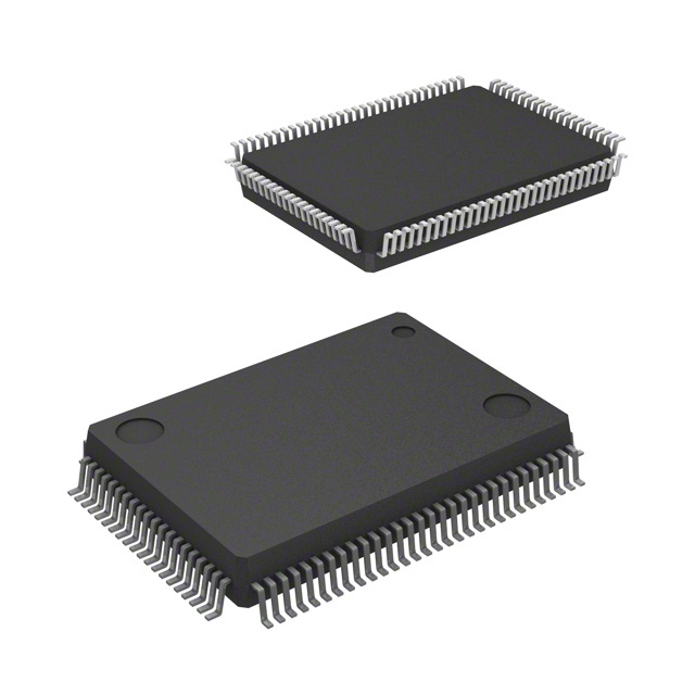
- Part No.:
- ATF1504AS-15QC100
- Manufacturer:
- Microchip Technology
- Package:
- 100-BQFP
- Datasheet:
-
 ATF1504AS-15QC100.pdf
- Description:
- IC CPLD 64MC 15NS 100QFP
- Quantity:
- Payment:

- Shipping:

Inventory:3,913
Please send an inquiry. Send us your inquiry, and we will respond immediately.
Product details
Overview
ATF1504AS-15QC100 from Microchip (formerly Atmel) is a high-density, electrically-erasable Complex Programmable Logic Device (CPLD) with 64 macrocells, 5 product terms per macrocell (expandable to 40), 7.5 ns pin-to-pin delay, 125 MHz registered operation, and 100-lead TQFP packaging. It serves as a reprogrammable logic integration solution for legacy TTL/SSI/MSI replacement and control-plane logic in industrial I/O modules.
For engineers reviewing the ATF1504AS-15QC100 datasheet, ATF1504AS-15QC100 pinout, ATF1504AS-15QC100 application, or ATF1504AS-15QC100 equivalent, this device delivers in-system programmability via JTAG, PCI-compliant I/O drive, flexible macrocell configuration (D/T/latch), and advanced power management including pin-controlled 1 mA standby mode - all critical for field-upgradable embedded control designs.
Technical Context
The ATF1504AS-15QC100 implements a global bus architecture feeding up to 40 signals into each logic block's switch matrix, enabling high routing density and successful pin-locked design iterations. Its 64 macrocells each generate buried feedback to the global bus and foldback terms to regional buses, supporting cascade logic chains with up to 40-product-term sum terms.
Each macrocell supports configurable flip-flops (D/T/JK/SR/latch) with clock sourced from global clocks (GCLK1–3) or individual product terms, asynchronous reset/preset, and output enable selectable per macrocell. ITD circuits on global clocks, inputs, and I/Os provide input transition detection for edge-sensitive control logic.
Key Specifications
| Parameter | Value and Actual Design Meaning |
|---|---|
| Logic Density | 64 macrocells - provides gate count equivalent to ~1500 usable PLD gates for medium-complexity control logic. |
| Timing Performance | 7.5 ns max pin-to-pin delay (–15 speed grade) - enables synchronous logic operation up to 125 MHz registered frequency. |
| I/O Count | Up to 68 bi-directional I/O pins + 4 dedicated inputs - supports dense board-level interfacing with minimal external glue logic. |
| Power Management | 1 mA standby mode (pin-controlled) and per-macrocell reduced-power bit - reduces dynamic and static power in low-activity states. |
| Programming Interface | JTAG ISP compliant with IEEE 1149.1-1990/1149.1a-1993 - allows in-circuit programming without device removal or special voltage rails. |
| Supply Voltage | 3.3 V or 5.0 V I/O-compatible (VCCIO), 5.0 V core (VCCINT) - supports mixed-voltage system integration and legacy 5 V TTL interoperability. |
| Security & Reliability | Programmable security fuse + 20-year data retention + 10,000 program/erase cycles - ensures IP protection and long-term field reliability. |
Pinout & Package
ATF1504AS-15QC100 is packaged in a 100-lead Thin Quad Flat Package (TQFP) with 0.5 mm pitch, RoHS-compliant, and rated for industrial temperature range (–40°C to +85°C). Pin functions include 68 I/Os, 4 dedicated inputs (GCLK1–3, GCLR), 2 power-down pins (PD1/PD2), JTAG interface (TCK/TMS/TDI/TDO), and dual-supply rails (VCCIO/VCCINT/GND).
| Pin/Terminal | Circuit Role | Design Meaning |
|---|---|---|
| GCLK1, GCLK2, GCLK3 | Global Clock Input | Three independent clock sources assignable per macrocell; supports synchronous logic with low skew across device. |
| GCLR | Global Clear Input | Asynchronous reset signal for all macrocell flip-flops; may be OR'd with product-term reset for selective clearing. |
| PD1, PD2 | Power-down Control | Active-high pins that force device into sub-10 mA power-down mode; latches internal state and holds outputs valid. |
| TCK, TMS, TDI, TDO | JTAG Boundary-scan Port | IEEE 1149.1-compliant test and programming interface; supports in-system programming and PCB interconnect testing. |
| VCCIO / VCCINT | Power Supply Rails | VCCIO powers I/O buffers (3.3 V or 5.0 V); VCCINT powers core logic (5.0 V); decoupling required per rail for noise immunity. |
Key Features
| Feature | Design Value |
|---|---|
| Flexible Macrocell Architecture | Each of 64 macrocells supports D/T/JK/SR flip-flop or transparent latch, with clock, reset, preset, and output enable individually assignable from global or product-term sources. |
| Enhanced Routing Resources | Global bus carries 68 I/O + 64 buried feedback signals; switch matrix selects up to 40 signals per logic block - increases logic utilization and routing success rate. |
| PCI-Compliant I/O Drive | High-current output drivers meet PCI electrical specs without parallel pin stacking - enables direct connection to PCI bus with low skew and noise control. |
| Programmable Slew Rate | Per-output slew rate control (fast/slow) reduces EMI and crosstalk on high-speed traces; defaults to slow for noise-sensitive applications. |
| Pin-keeper Circuits | Configurable keeper on all inputs/I/Os prevents floating states and eliminates need for external pull-ups - saves board space and reduces DC power loss. |
Applications
| Industrial PLC I/O Expansion | Legacy System Glue Logic Replacement |
|---|---|
Use Scenario: Adding isolated digital input/output channels to programmable logic controller backplanes with strict timing and noise requirements. IC Role / Device Role / Timing Role: Configurable logic engine implementing debounce, edge detection, and protocol translation between field sensors and CPU bus. Use Value: Replaces multiple 74-series TTL chips with single reprogrammable device; JTAG ISP enables firmware updates without hardware change. |
Use Scenario: Modernizing aging test equipment control boards originally built with discrete PALs and GALs. IC Role / Device Role / Timing Role: Drop-in CPLD substitute for obsolete 22V10/16V8 devices, preserving pinout while adding debug visibility via JTAG BST. Use Value: Maintains original PCB layout; 7.5 ns propagation delay meets legacy timing budgets; security fuse protects reverse-engineered logic. |
| PCI Bus Interface Controller | Field-Upgradeable Communication Module |
Use Scenario: Implementing address decoding, burst control, and parity generation for add-in cards in PCI-based instrumentation systems. IC Role / Device Role / Timing Role: PCI-compliant logic block managing command handshaking, data strobing, and error signaling on 32-bit/33 MHz bus. Use Value: Meets PCI spec for drive strength and skew; programmable slew rate minimizes signal integrity issues on shared bus segments. |
Use Scenario: Enabling remote firmware patching of RS-485 gateway modules deployed in distributed SCADA networks. IC Role / Device Role / Timing Role: Reconfigurable state machine handling protocol conversion (Modbus RTU ↔ ASCII) and watchdog supervision. Use Value: In-system programmability allows logic updates over serial link; 1 mA standby mode extends battery life in solar-powered nodes. |
Equivalent & Alternatives
The following parts are listed as comparable options for similar CPLD applications.
| Alternative Part | Technical Difference | Application Difference | Selection Advice |
|---|---|---|---|
| XCR3064XL-10VQ100C | 64 macrocells, 10 ns speed, 3.3 V only, CoolRunner-II architecture with lower static current (10 µA typical) | Lacks 5 V I/O tolerance and PCI drive; better suited for ultra-low-power battery applications than industrial 5 V systems | Select when 3.3 V-only operation and lowest possible ICC1 are prioritized over legacy voltage compatibility. |
| EPM3064ATC100-10 | 64 macrocells, 10 ns speed, 3.3 V core/IO, MAX 3000A family with higher pin count flexibility but no JTAG boundary-scan | No IEEE 1149.1 support; requires external programmer; lacks pin-keeper and ITD features | Choose when cost sensitivity outweighs field-programmability and testability requirements. |
Compared with XCR3064XL-10VQ100C and EPM3064ATC100-10, the ATF1504AS-15QC100 uniquely combines 5 V/3.3 V I/O compatibility, PCI-compliant drive, JTAG boundary-scan, and pin-keeper circuits - making it the only option among the three suitable for retrofitting legacy 5 V industrial controllers with field-upgrade capability.
Availability
ATF1504AS-15QC100 is available at Aetrix Electronics and suitable for industrial PLC I/O expansion, legacy system glue logic replacement, and PCI bus interface controller applications requiring stable component supply and long-term lifecycle support.
Supply support for ATF1504AS-15QC100 includes scheduled delivery planning, volume procurement assistance, BOM continuity management, traceable sourcing, and lifecycle availability coordination for OEM customers, industrial embedded developers, connected-device designers, and electronics production programs.
Manufacturer
Microchip Technology acquired Atmel in 2016 and continues to support its legacy PLD portfolio, including the ATF1504AS family, with full documentation, programming tools, and long-term availability commitments.
The ATF1504AS series was designed specifically for high-reliability, field-upgradable control logic in industrial automation, test equipment, and communications infrastructure - emphasizing in-system programmability, mixed-voltage I/O, and robust power management.
FAQ
What is the maximum operating frequency of the ATF1504AS-15QC100?
The ATF1504AS-15QC100 supports registered operation up to 125 MHz, as confirmed by its –15 speed grade rating and tCNT = 8 ns minimum global clock period. This frequency applies to synchronous logic paths using global clocks GCLK1–3; combinatorial paths achieve 7.5 ns pin-to-pin delay. The actual achievable system frequency depends on design complexity, routing, and timing closure achieved during fitting.
Does the ATF1504AS-15QC100 support both 3.3 V and 5.0 V I/O interfaces?
Yes, the ATF1504AS-15QC100 supports dual-voltage I/O operation: VCCIO may be set to either 3.0–3.6 V or 4.75–5.25 V, while VCCINT remains fixed at 5.0 V ±5%. This allows direct interfacing with both modern 3.3 V microcontrollers and legacy 5 V TTL/CMOS logic without level shifters - a key advantage for system upgrades.
How does the pin-keeper feature work on the ATF1504AS-15QC100?
The ATF1504AS-15QC100 includes programmable pin-keeper circuits on all inputs and I/Os. When enabled, these circuits retain the last driven logic state (high or low) after the driving source is removed, preventing floating inputs that cause shoot-through current and noise. This eliminates external pull-up resistors and associated DC power loss - especially valuable in high-pin-count industrial I/O designs.
Can the ATF1504AS-15QC100 be programmed in-system without removing it from the PCB?
Yes, the ATF1504AS-15QC100 is fully in-system programmable (ISP) via its 4-pin JTAG interface (TCK/TMS/TDI/TDO), compliant with IEEE Std. 1149.1-1990 and 1149.1a-1993. Programming can be performed using standard JTAG tools, Atmel-provided utilities, or third-party ATE systems - enabling field firmware updates and manufacturing programming without device removal.
What is the purpose of the PD1 and PD2 pins on the ATF1504AS-15QC100?
PD1 and PD2 are dedicated power-down control pins on the ATF1504AS-15QC100. When asserted high (with power-down mode enabled in the design file), either pin forces the device into a sub-10 mA standby state while latching all internal registers and maintaining valid output levels. These pins cannot serve as general-purpose logic inputs when power-down is active, but their macrocell resources remain usable for foldback/cascade logic.
ATF1504AS-15QC100 Specifications
- Product attributes
- Attribute value
- Manufacturer:
- Microchip Technology
- Series:
- ATF15xx
- Package/Case:
- 100-BQFP
- Packaging:
- Tray
- Product Status:
- Obsolete
- Programmable:
- Not Verified
- Programmable Type:
- In System Programmable (min 10K program/erase cycles)
- Delay Time tpd(1) Max:
- 15 ns
- Voltage Supply - Internal:
- 4.75V ~ 5.25V
- Number of Logic Elements/Blocks:
- -
- Number of Macrocells:
- 64
- Number of Gates:
- -
- Number of I/O:
- 64
- Operating Temperature:
- 0°C ~ 70°C (TA)
- Grade:
- -
- Qualification:
- -
- Mounting Type:
- Surface Mount
- Supplier Device Package:
- 100-PQFP (14x20)
ATF1504AS-15QC100 FAQ
1.How can I place an order for ATF1504AS-15QC100 through Aetrix?
Please submit a Request for Quotation (RFQ) for ATF1504AS-15QC100 on Aetrix. Our sales agent will provide a competitive quotation and guide you through the order confirmation once you accept the terms.
2.Are the price and stock information for ATF1504AS-15QC100 reliable?
The price and inventory of ATF1504AS-15QC100 are updated periodically and may fluctuate due to market conditions. Stock and pricing data are typically refreshed every 24 hours. Quotation validity for ATF1504AS-15QC100 is usually 5 days.
3.What payment methods are accepted for ATF1504AS-15QC100?
We accept Wire Transfer, PayPal, Credit Card, Western Union, MoneyGram, and Escrow for ATF1504AS-15QC100 transactions.
Note: Certain payment methods may incur a processing fee.
4.How is shipping managed for ATF1504AS-15QC100?
ATF1504AS-15QC100 orders can be shipped via leading logistics carriers, including DHL, UPS, FedEx, TNT, or Registered Mail.
Once your ATF1504AS-15QC100 order is processed, you will receive an email with the shipment details and tracking number.
Note: Tracking information may take up to 24 hours to appear. Express delivery typically takes 3–5 business days.
5.How can I obtain technical support or documentation for ATF1504AS-15QC100?
For technical support, including ATF1504AS-15QC100 datasheets, pinout diagrams, or application guidance, please contact our engineering support team. They can provide detailed documentation and assistance for your ATF1504AS-15QC100 requirements.
6.How does Aetrix verify that ATF1504AS-15QC100 is sourced from the original manufacturer or authorized distributors?
All ATF1504AS-15QC100 products on Aetrix are procured from qualified distributors and authorized channels. Our dedicated quality assurance team conducts strict verification, including traceability checks and, if necessary, third-party testing. This ensures that ATF1504AS-15QC100 meets industry standards.
7.What is the process for return or replacement of ATF1504AS-15QC100?
All ATF1504AS-15QC100 units undergo pre-shipment inspection (PSI). If there is an issue with ATF1504AS-15QC100, returns or replacements are accepted under the following conditions:
1.Quantity discrepancies, incorrect items, or visible external defects (such as breakage or corrosion), acknowledged by Aetrix.
2.The issue is reported within 90 days of delivery.
3.The ATF1504AS-15QC100 part is unused and in its original packaging.
Return procedure for ATF1504AS-15QC100:
1.Submit a request within 90 days.
2.Obtain a Return Material Authorization (RMA) from Aetrix.
ATF1504AS-15QC100 Tags
-
5M40ZE64C5N
Intel
-
ATF1502ASV-15AU44
Microchip Technology
-
5M80ZE64C5N
Intel
-
5M80ZT100C5N
Intel
-
ATF1502AS-10AU44
Microchip Technology
-
ATF1502AS-10JU44
Microchip Technology
-
5M80ZE64I5N
Intel
-
5M80ZT100I5N
Intel
-
LC4032V-75TN48C
Lattice Semiconductor Corporation
-
ATF1504ASV-15AU44
Microchip Technology
-
ATF1504AS-10JU44
Microchip Technology
-
5M160ZE64C5N
Intel
Tech Hub

TTL and CMOS logic families differ in thresholds, loading, output drive, power and timing. This engineering guide compares 74HC and 74HCT, calculates noise margins and checks 3.3 V/5 V compatibility.

A practical engineering guide to 3.3V and 5V logic compatibility, input thresholds, resistor dividers, translator ICs, MOSFET level shifting, I2C pull-ups, timing limits and power-sequencing risks.

The 74HC595 uses push-pull logic outputs, while the TPIC6B595 uses 50 V open-drain DMOS sinks for higher-power loads. This guide compares timing, current limits, 3.3 V interfacing, load wiring, thermal…

The 74HC595 converts serial data into eight stable parallel outputs. This guide covers pin functions, shift and storage timing, OE and MR behavior, drive-current limits, cascading, voltage compatibilit…

A technical comparison of level-sensitive latches and edge-triggered flip-flops, covering timing windows, setup and hold limits, master–slave operation, time borrowing, race-through, HDL inference and…

A D latch stores one bit while Enable controls when data can pass. This reference covers gate-level operation, truth tables, transparency, setup and hold timing, LE versus OE, common ICs and practical …

An SR latch stores one bit through cross-coupled feedback. This engineering reference covers NOR and NAND implementations, truth tables, forbidden-state recovery, gated operation, switch debouncing, fa…

Latch circuits retain one bit through feedback. This technical reference covers SR and D latches, truth tables, transparency, timing limits, latch-versus-flip-flop behavior, applications and common log…

An engineering guide to LED driver operation, constant-current and constant-voltage outputs, linear and switching topologies, dimming, IC selection, calculations, replacement compatibility, and fault c…

Operational amplifier guide covering op amp basics, feedback, ideal vs real op amps, common configurations, buffer circuits, offset, bias current, gain-bandwidth, slew rate, rail-to-rail limits and sel…


