
 My Inquiry
 My Account


Microchip Technology ATF1504ASVL-20JU44
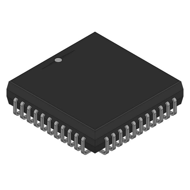
- Part No.:
- ATF1504ASVL-20JU44
- Manufacturer:
- Microchip Technology
- Package:
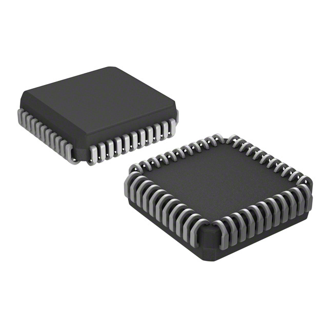
- 44-LCC (J-Lead)
- Datasheet:
-
 ATF1504ASVL-20JU44.pdf
- Description:
- IC CPLD 64MC 20NS 44PLCC
- Quantity:
- Payment:

- Shipping:

Inventory:4,644
Please send an inquiry. Send us your inquiry, and we will respond immediately.
Product details
Overview
ATF1504ASVL-20JU44 from Microchip Technology is a 3.3V, 64-macrocell Complex Programmable Logic Device (CPLD) in 44-lead PLCC package, featuring 15 ns maximum pin-to-pin delay, 77 MHz registered operation, and automatic 5 µA standby current. It supports in-system programming via JTAG and integrates logic from TTL, SSI, MSI, LSI, and classic PLDs in industrial temperature applications.
For engineers reviewing the ATF1504ASVL-20JU44 datasheet, ATF1504ASVL-20JU44 pinout, ATF1504ASVL-20JU44 application, or ATF1504ASVL-20JU44 equivalent, key selection criteria include its 3.0–3.6V supply range, JTAG boundary-scan compliance (IEEE 1149.1), PCI compatibility, programmable slew rate, and dual power-down pins (PD1/PD2) for low-power system control.
Technical Context
The ATF1504ASVL-20JU44 implements a flexible macrocell architecture with five product terms per macrocell-expandable to 40 via cascade logic-and supports D/T/latch flip-flops, transparent-latch mode, and combinatorial outputs with registered feedback. Its global bus feeds all 64 macrocells and I/Os, enabling up to 40 signal selections per logic block.
It features three global clock inputs (GCLK1–GCLK3), input transition detection (ITD) on clocks and I/Os, fast registered input from product terms, and programmable pin-keeper circuits. Power management includes edge-controlled standby (5 µA typ.), per-macrocell reduced-power mode, and pin-controlled power-down (<5 mA).
Key Specifications
| Parameter | Value and Actual Design Meaning |
|---|---|
| Logic Density | 64 macrocells with 5 base + up to 40 expandable product terms per macrocell for high-complexity logic synthesis |
| Timing Performance | 15 ns max pin-to-pin delay; 77 MHz max registered operation frequency at -20 speed grade |
| Supply Voltage | 3.0 V to 3.6 V - compatible with 3.3V TTL/CMOS systems and PCI signaling standards |
| Standby Current | 5 µA typical - automatically entered during logic inactivity, reducing idle power in battery-sensitive designs |
| JTAG Compliance | Fully supports IEEE Std. 1149.1-1990/1149.1a-1993 for boundary-scan testing and ISP programming |
| Package | 44-lead PLCC (JU44) - through-hole mountable, RoHS-compliant, with 32 user I/O pins and 4 dedicated control inputs |
| Operating Temperature | -40°C to +85°C - qualified for industrial environments without derating |
Pinout & Package
ATF1504ASVL-20JU44 is housed in a 44-lead Plastic Leaded Chip Carrier (PLCC) package with J-lead configuration. Pin 1 is located at the index corner (notch side, top-left when viewed from top); leads are numbered counter-clockwise.
| Pin/Terminal | Circuit Role | Design Meaning |
|---|---|---|
| 1 (TDI/I/O) | JTAG Test Data Input / General I/O | Primary serial input for ISP programming and boundary-scan data; configurable as logic I/O if JTAG disabled |
| 7 (I/O/TMS) | JTAG Test Mode Select / General I/O | Selects TAP controller state; retains full I/O functionality when JTAG not enabled |
| 26 (I/O/TCK) | JTAG Test Clock / General I/O | Drives TAP state transitions; operates at system clock rates up to 25 MHz for reliable ISP |
| 32 (I/O/TDO) | JTAG Test Data Output / General I/O | Serial output for scan-out data; high-impedance when not active in BST mode |
| 5, 19 (PD1/I/O, PD2/I/O) | Power-Down Control / General I/O | Asserting either pin high enters <5 mA power-down mode; disables logic but holds register and output states |
| 37–40 (GCLK1/I, GCLR/I, OE1/I, GCLK2/OE2/I) | Dedicated Global Control Inputs | Fixed-function pins for clock, asynchronous clear, and output enable - not reassignable as general I/O |
| 35 (GCLK3/I/O) | Global Clock 3 / Bidirectional I/O | Third global clock input; also usable as standard I/O when not assigned as clock |
| 4, 16, 24, 36 (GND) | Ground Reference | Four independent ground connections reduce noise coupling and improve signal integrity across logic blocks |
| 9, 17, 29, 41 (VCC) | Power Supply | Four VCC (VCCINT/VCCIO) pins ensure stable 3.3V distribution to core and I/O circuitry |
Key Features
| Feature | Design Value |
|---|---|
| Programmable Slew Rate | Per-output switching speed control reduces EMI and crosstalk on high-speed buses without external termination |
| Pin-Keeper Circuits | Prevents floating inputs/I/Os by latching last driven state - eliminates need for external pull-ups and saves board space |
| Three Global Clock Pins | Enables multi-domain synchronous design (e.g., control, data, interface clocks) without consuming macrocell resources |
| Input Transition Detection (ITD) | Hardware-level edge detection on clocks, inputs, and I/Os enables glitch-free asynchronous event capture and wake-on-interrupt |
| VCC Power-Up Reset | Monotonic VCC-triggered initialization ensures deterministic state machine startup and avoids metastability at power-on |
| Security Fuse | One-time programmable fuse prevents unauthorized readback of configuration bitstream while preserving 16-bit User Signature access |
Applications
| Industrial PLC I/O Expansion | Legacy Bus Interface Adapter |
|---|---|
Use Scenario: Adding isolated digital I/O channels to programmable logic controllers using 24V DC field signals. IC Role / Device Role / Timing Role: CPLD implements level-shifting, debounce, and parallel-to-serial conversion between field-side optocouplers and microcontroller SPI bus. Use Value: 64 macrocells support >32-channel I/O expansion with <15 ns response latency and automatic standby during idle cycles. |
Use Scenario: Bridging ISA or PCI bus peripherals to modern ARM-based controllers in test equipment upgrades. IC Role / Device Role / Timing Role: Glue logic translates address/data strobes, manages wait-state insertion, and handles PCI compliance timing (setup/hold, tCL/tCH). Use Value: PCI-compliant timing, 3.3V tolerance, and JTAG debug visibility enable drop-in replacement without FPGA toolchain dependency. |
| Automotive Body Control Module | Medical Device Safety Monitor |
Use Scenario: Centralized control of lighting, door locks, and window motors in 12V automotive systems with CAN coordination. IC Role / Device Role / Timing Role: State-machine-based sequencer synchronizes actuator drivers, monitors switch inputs, and asserts fault flags to main MCU over discrete lines. Use Value: -40°C to +85°C rating, 200 mA latch-up immunity, and programmable pin-keepers ensure robust operation in under-hood environments. |
Use Scenario: Real-time monitoring of redundant sensor inputs (e.g., pressure, temperature) in Class II medical devices with fail-safe shutdown. IC Role / Device Role / Timing Role: Hardware-level voting logic compares dual sensors and triggers immediate hardware reset if mismatch exceeds threshold. Use Value: Deterministic <15 ns propagation, security fuse protection of safety-critical configuration, and 20-year EEPROM retention meet IEC 62304 requirements. |
Equivalent & Alternatives
The following parts are listed as comparable options for similar CPLD applications.
| Alternative Part | Technical Difference | Application Difference | Selection Advice |
|---|---|---|---|
| XCR3064XL-10VQ44C | 64-macrocell CoolRunner-II CPLD; 3.3V supply; 10 ns tPD; no automatic standby (min ICC = 25 µA) | Lacks integrated ITD, pin-keeper, and VCC power-up reset; requires external reset IC | Preferred where ultra-low static power is secondary to higher speed margin and Xilinx toolchain familiarity |
| ATF1508ASVL-20JU44 | Same family, 128-macrocell variant in identical 44-lead PLCC; same 5 µA standby, JTAG, and feature set | Provides double logic density without PCB change - suitable for design scalability or future-proofing | Select when additional macrocells are needed for expanded I/O mapping or complex state machines without layout revision |
Compared with XCR3064XL-10VQ44C, ATF1504ASVL-20JU44 delivers 5× lower standby current and integrated safety features (ITD, pin-keeper, power-up reset); versus ATF1508ASVL-20JU44, it offers cost and power optimization for designs that fully utilize only 64 macrocells.
Availability
ATF1504ASVL-20JU44 is available at Aetrix Electronics and suitable for industrial PLC I/O expansion, legacy bus interface adapters, and automotive body control modules requiring stable component supply across long production lifecycles.
Supply support for ATF1504ASVL-20JU44 includes scheduled delivery planning, volume procurement assistance, BOM continuity management, traceable sourcing, and lifecycle availability coordination for OEM customers, industrial embedded developers, connected-device designers, and electronics production programs.
Manufacturer
Microchip Technology is a U.S.-based semiconductor manufacturer specializing in microcontrollers, analog devices, and programmable logic solutions with broad industrial and automotive qualification.
The ATF1504ASVL series targets cost-sensitive, high-reliability embedded control applications where in-system programmability, low-power operation, and long-term supply stability are critical design requirements.
FAQ
What is the operating voltage range for ATF1504ASVL-20JU44?
The ATF1504ASVL-20JU44 operates from 3.0 V to 3.6 V. This 3.3V nominal range ensures compatibility with PCI signaling standards and common industrial 3.3V power rails. Operation outside this range may cause functional failure or permanent damage, as specified in Absolute Maximum Ratings. The device's internal regulators and logic thresholds are optimized exclusively for this voltage window.
Does ATF1504ASVL-20JU44 support in-system programming (ISP)?
Yes, ATF1504ASVL-20JU44 supports full in-system programming via its 4-pin JTAG interface compliant with IEEE Std. 1149.1. Programming can be performed without removing the device from the PCB using standard SVF files. The JTAG pins (TDI, TMS, TCK, TDO) are configurable as general I/O when ISP is disabled in the design file.
How does the automatic standby mode work in ATF1504ASVL-20JU44?
The ATF1504ASVL-20JU44 automatically enters a 5 µA standby mode when no logic transitions occur - detected via internal activity monitoring. This feature provides proportional power savings in low-activity systems (e.g., <5 MHz clock domains) without software intervention. Standby exits immediately upon first signal transition, restoring full operation with no latency penalty.
What are the functions of the PD1 and PD2 pins on ATF1504ASVL-20JU44?
PD1 and PD2 are dedicated power-down control inputs on ATF1504ASVL-20JU44. When either pin is driven high (with power-down mode enabled in the design), the device enters a <5 mA power-down state: internal logic and outputs are latched, I/Os retain their last state via pin-keeper circuits, and all inputs except PD pins are ignored. These pins cannot serve as logic I/O when power-down is active.
Is ATF1504ASVL-20JU44 RoHS compliant and lead-free?
Yes, ATF1504ASVL-20JU44 is Green (Pb/Halide-Free/RoHS Compliant) per Microchip's DS20006185A datasheet. The 44-lead PLCC package uses lead-free terminations and complies with EU Directive 2011/65/EU. No lead content is present in solderable surfaces or internal die attach materials, and the device meets JEDEC J-STD-020 moisture sensitivity level MSL-3.
ATF1504ASVL-20JU44 Specifications
- Product attributes
- Attribute value
- Manufacturer:
- Microchip Technology
- Series:
- ATF15xx
- Package/Case:
- 44-LCC (J-Lead)
- Packaging:
- Tube
- Product Status:
- Active
- Programmable:
- Verified
- Programmable Type:
- In System Programmable (min 10K program/erase cycles)
- Delay Time tpd(1) Max:
- 20 ns
- Voltage Supply - Internal:
- 3V ~ 3.6V
- Number of Logic Elements/Blocks:
- -
- Number of Macrocells:
- 64
- Number of Gates:
- -
- Number of I/O:
- 32
- Operating Temperature:
- -40°C ~ 85°C (TA)
- Grade:
- -
- Qualification:
- -
- Mounting Type:
- Surface Mount
- Supplier Device Package:
- 44-PLCC (16.6x16.6)
ATF1504ASVL-20JU44 FAQ
1.How can I place an order for ATF1504ASVL-20JU44 through Aetrix?
Please submit a Request for Quotation (RFQ) for ATF1504ASVL-20JU44 on Aetrix. Our sales agent will provide a competitive quotation and guide you through the order confirmation once you accept the terms.
2.Are the price and stock information for ATF1504ASVL-20JU44 reliable?
The price and inventory of ATF1504ASVL-20JU44 are updated periodically and may fluctuate due to market conditions. Stock and pricing data are typically refreshed every 24 hours. Quotation validity for ATF1504ASVL-20JU44 is usually 5 days.
3.What payment methods are accepted for ATF1504ASVL-20JU44?
We accept Wire Transfer, PayPal, Credit Card, Western Union, MoneyGram, and Escrow for ATF1504ASVL-20JU44 transactions.
Note: Certain payment methods may incur a processing fee.
4.How is shipping managed for ATF1504ASVL-20JU44?
ATF1504ASVL-20JU44 orders can be shipped via leading logistics carriers, including DHL, UPS, FedEx, TNT, or Registered Mail.
Once your ATF1504ASVL-20JU44 order is processed, you will receive an email with the shipment details and tracking number.
Note: Tracking information may take up to 24 hours to appear. Express delivery typically takes 3–5 business days.
5.How can I obtain technical support or documentation for ATF1504ASVL-20JU44?
For technical support, including ATF1504ASVL-20JU44 datasheets, pinout diagrams, or application guidance, please contact our engineering support team. They can provide detailed documentation and assistance for your ATF1504ASVL-20JU44 requirements.
6.How does Aetrix verify that ATF1504ASVL-20JU44 is sourced from the original manufacturer or authorized distributors?
All ATF1504ASVL-20JU44 products on Aetrix are procured from qualified distributors and authorized channels. Our dedicated quality assurance team conducts strict verification, including traceability checks and, if necessary, third-party testing. This ensures that ATF1504ASVL-20JU44 meets industry standards.
7.What is the process for return or replacement of ATF1504ASVL-20JU44?
All ATF1504ASVL-20JU44 units undergo pre-shipment inspection (PSI). If there is an issue with ATF1504ASVL-20JU44, returns or replacements are accepted under the following conditions:
1.Quantity discrepancies, incorrect items, or visible external defects (such as breakage or corrosion), acknowledged by Aetrix.
2.The issue is reported within 90 days of delivery.
3.The ATF1504ASVL-20JU44 part is unused and in its original packaging.
Return procedure for ATF1504ASVL-20JU44:
1.Submit a request within 90 days.
2.Obtain a Return Material Authorization (RMA) from Aetrix.
ATF1504ASVL-20JU44 Tags
-
5M40ZE64C5N
Intel
-
ATF1502ASV-15AU44
Microchip Technology
-
5M80ZE64C5N
Intel
-
5M80ZT100C5N
Intel
-
ATF1502AS-10AU44
Microchip Technology
-
ATF1502AS-10JU44
Microchip Technology
-
5M80ZE64I5N
Intel
-
5M80ZT100I5N
Intel
-
LC4032V-75TN48C
Lattice Semiconductor Corporation
-
ATF1504ASV-15AU44
Microchip Technology
-
ATF1504AS-10JU44
Microchip Technology
-
5M160ZE64C5N
Intel
Tech Hub

TTL and CMOS logic families differ in thresholds, loading, output drive, power and timing. This engineering guide compares 74HC and 74HCT, calculates noise margins and checks 3.3 V/5 V compatibility.

A practical engineering guide to 3.3V and 5V logic compatibility, input thresholds, resistor dividers, translator ICs, MOSFET level shifting, I2C pull-ups, timing limits and power-sequencing risks.

The 74HC595 uses push-pull logic outputs, while the TPIC6B595 uses 50 V open-drain DMOS sinks for higher-power loads. This guide compares timing, current limits, 3.3 V interfacing, load wiring, thermal…

The 74HC595 converts serial data into eight stable parallel outputs. This guide covers pin functions, shift and storage timing, OE and MR behavior, drive-current limits, cascading, voltage compatibilit…

A technical comparison of level-sensitive latches and edge-triggered flip-flops, covering timing windows, setup and hold limits, master–slave operation, time borrowing, race-through, HDL inference and…

A D latch stores one bit while Enable controls when data can pass. This reference covers gate-level operation, truth tables, transparency, setup and hold timing, LE versus OE, common ICs and practical …

An SR latch stores one bit through cross-coupled feedback. This engineering reference covers NOR and NAND implementations, truth tables, forbidden-state recovery, gated operation, switch debouncing, fa…

Latch circuits retain one bit through feedback. This technical reference covers SR and D latches, truth tables, transparency, timing limits, latch-versus-flip-flop behavior, applications and common log…

An engineering guide to LED driver operation, constant-current and constant-voltage outputs, linear and switching topologies, dimming, IC selection, calculations, replacement compatibility, and fault c…

Operational amplifier guide covering op amp basics, feedback, ideal vs real op amps, common configurations, buffer circuits, offset, bias current, gain-bandwidth, slew rate, rail-to-rail limits and sel…


