
 My Inquiry
 My Account


Microchip Technology ATMEGA128RFA1-ZUR00
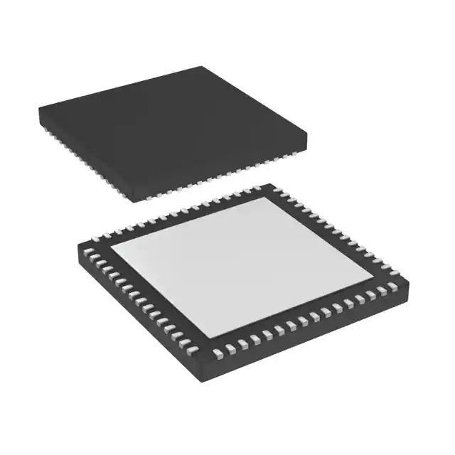
- Part No.:
- ATMEGA128RFA1-ZUR00
- Manufacturer:
- Microchip Technology
- Category:
- RF Transceiver ICs
- Package:
- 64-VFQFN Exposed Pad
- Datasheet:
-
 ATMEGA128RFA1-ZUR00.pdf
- Description:
- IC RF TXRX+MCU 802.15.4 64QFN
- Quantity:
- Payment:

- Shipping:

Inventory:3,985
Please send an inquiry. Send us your inquiry, and we will respond immediately.
Product details
Overview
ATMEGA128RFA1-ZUR00 from Microchip Technology (formerly Atmel) is an 8-bit AVR microcontroller with integrated 2.4 GHz IEEE 802.15.4/ZigBee transceiver, 128 KB Flash, 16 KB SRAM, and hardware AES encryption. It operates from 1.8–3.6 V, achieves 16 MIPS at 16 MHz, and supports ultra-low-power Deep Sleep mode (<250 nA). It targets battery-powered wireless sensor nodes in industrial monitoring and smart home gateways.
For engineers reviewing the ATMEGA128RFA1-ZUR00 datasheet, ATMEGA128RFA1-ZUR00 pinout, ATMEGA128RFA1-ZUR00 application, or ATMEGA128RFA1-ZUR00 equivalent, key selection criteria include its monolithic 2.4 GHz transceiver performance (–100 dBm RX sensitivity, +3.5 dBm TX), integrated voltage regulation, 38 programmable I/O lines, and IEEE 802.15.4 MAC hardware acceleration.
Technical Context
The ATMEGA128RFA1-ZUR00 integrates a RISC-based AVR CPU core with a fully featured 2.4 GHz DSSS transceiver supporting data rates up to 2 Mb/s. Its radio subsystem includes hardware-assisted MAC (auto-acknowledge, auto-retry), 32-bit IEEE 802.15.4 symbol counter, and baseband processing (spreading/despreading, CRC-16).
It features dual crystal oscillators (16 MHz for RF/microcontroller, 32.768 kHz for low-power timing), on-chip analog regulators (AVDD/DVDD), and dedicated RF ground pins (AVSS_RFP/AVSS_RFN). The device implements six software-selectable power-save modes, including Deep Sleep with active 32.768 kHz oscillator and MAC symbol counter.
Key Specifications
| Parameter | Value and Actual Design Meaning |
|---|---|
| Core Architecture | AVR 8-bit RISC with 135 instructions; most execute in one cycle for deterministic real-time control. |
| Flash Memory | 128 KB In-System Self-Programmable Flash with read-while-write capability for firmware updates over-the-air. |
| Transceiver Data Rates | 250 kb/s, 500 kb/s, 1 Mb/s, and 2 Mb/s - selectable per IEEE 802.15.4-2011 PHY layer requirements. |
| RX Sensitivity | –100 dBm at 250 kb/s - enables robust link budget in noisy industrial environments. |
| TX Output Power | Up to +3.5 dBm - sufficient for 100+ meter line-of-sight range with standard PCB antenna. |
| Supply Current (Deep Sleep) | <250 nA at 25°C - extends coin-cell battery life to multi-year operation in wake-on-RX applications. |
| Operating Voltage | 1.8–3.6 V with internal regulators - eliminates need for external LDOs in compact designs. |
| Temperature Range | –40°C to +125°C industrial grade - qualified for deployment in uncontrolled outdoor enclosures. |
Pinout & Package
ATMEGA128RFA1-ZUR00 uses a 64-pad QFN package (RoHS/Fully Green) with exposed metal thermal pad internally connected to AVSS. The pad must be soldered to PCB ground plane for mechanical stability and thermal performance.
| Pin/Terminal | Circuit Role | Design Meaning |
|---|---|---|
| RFP / RFN | Differential RF I/O port | Direct connection to balun or RF switch; requires impedance-matched 100 Ω differential layout. |
| XTAL1 / XTAL2 | 16 MHz crystal oscillator interface | Drives both RF transceiver and MCU core; requires low-parasitic 12 pF load capacitors. |
| AVSS_RFP / AVSS_RFN | Dedicated RF ground returns | Must be routed separately to minimize noise coupling into analog RF front-end. |
| DEVDD / EVDD | Digital and analog external supply inputs | Accept 1.8–3.6 V; feed internal regulators generating DVDD and AVDD for digital/analog domains. |
| TST / CLKI | Programming enable and external clock input | TST must be tied low if not used; CLKI allows external clock source instead of crystal. |
| PG0 / PF3–PF7 | GPIO with alternate functions (DIG3/DIG4, JTAG, ADC) | Support RF activity indicators (DIG3/DIG4) and boundary-scan debug without additional pins. |
Key Features
| Feature | Design Value |
|---|---|
| Hardware AES-128 Engine | Accelerates encryption/decryption for ZigBee Pro and 6LoWPAN security stacks without CPU overhead. |
| Integrated 32.768 kHz Oscillator | Enables sub-1 µA real-time clock and MAC symbol counter operation during Deep Sleep mode. |
| On-Chip Voltage Regulators | Generates clean, isolated DVDD and AVDD from single 1.8–3.6 V supply - reduces BOM count by two LDOs. |
| Hardware MAC Acceleration | Offloads frame filtering, auto-ACK, auto-retry, and CRC-16 computation from firmware - improves throughput and determinism. |
| Antenna Diversity Support | Uses PG1 (DIG1) and PF2 (DIG2) to control external RF switches - enhances link reliability in multipath environments. |
| True Random Number Generator | Provides entropy source for secure key generation compliant with FIPS 140-2 cryptographic requirements. |
Applications
| Smart Energy Meters | ZigBee Home Automation Hubs |
|---|---|
Use Scenario: Two-way communication between utility meter and concentrator using ZigBee SE profile. IC Role / Device Role / Timing Role: Full Function Device (FFD) executing ZigBee stack, managing time-sync via 32.768 kHz oscillator, and handling AES-secured payload encryption. Use Value: Single-chip solution eliminates discrete transceiver + MCU integration effort; Deep Sleep current <250 nA enables 10+ year battery life in tamper-detection mode. | Use Scenario: Central coordinator node aggregating sensor data from lighting, HVAC, and security endpoints. IC Role / Device Role / Timing Role: FFD with hardware MAC acceleration managing up to 65,000 devices; uses 16 MHz crystal for precise CSMA-CA timing. Use Value: Integrated 2.4 GHz transceiver with –100 dBm sensitivity ensures reliable mesh formation in dense residential RF environments. |
| Industrial Wireless Sensor Nodes | 6LoWPAN Border Routers |
Use Scenario: Battery-powered temperature/humidity node in factory floor with metal obstructions. IC Role / Device Role / Timing Role: Reduced Function Device (RFD) with antenna diversity (PG1/PF2) switching between two PCB traces to mitigate multipath fading. Use Value: Hardware diversity control avoids firmware latency; +3.5 dBm TX output compensates for 15–20 dB path loss in industrial settings. | Use Scenario: IPv6 gateway bridging IEEE 802.15.4 mesh network to Ethernet/Wi-Fi infrastructure. IC Role / Device Role / Timing Role: FFD running 6LoWPAN adaptation layer; leverages 128 KB Flash for CoAP server and TLS stack. Use Value: On-chip AES engine secures DTLS handshakes; 16 KB SRAM accommodates multiple concurrent IPv6 neighbor cache entries. |
Equivalent & Alternatives
The following parts are listed as comparable options for similar 2.4 GHz wireless microcontroller applications.
| Alternative Part | Technical Difference | Application Difference | Selection Advice |
|---|---|---|---|
| ATMEGA256RFR2-ZUR | 256 KB Flash, same 2.4 GHz transceiver IP, but no hardware AES; supports only 250/500 kb/s data rates. | Lacks AES acceleration - unsuitable for ZigBee Pro or secure 6LoWPAN deployments requiring link-layer encryption. | Select when larger code space is needed and security is handled at application layer or via external crypto IC. |
| CC2652R1FIPNR | ARM Cortex-M4F core, 352 KB Flash, integrated RF front-end, supports BLE 5.0 and IEEE 802.15.4 simultaneously. | Dual-mode radio requires different stack licensing and has higher active current (5.9 mA RX vs 12.5 mA for ATMEGA128RFA1-ZUR00). | Select for multi-protocol gateways or where ARM ecosystem tooling and BLE coexistence are required. |
Compared with ATMEGA256RFR2-ZUR and CC2652R1FIPNR, the ATMEGA128RFA1-ZUR00 delivers optimal balance of legacy AVR toolchain support, hardware AES for ZigBee compliance, and ultra-low Deep Sleep current - making it ideal for cost-sensitive, long-life, standards-certified wireless sensor nodes.
Availability
ATMEGA128RFA1-ZUR00 is available at Aetrix Electronics and suitable for smart energy metering, ZigBee home automation hubs, and industrial wireless sensor networks requiring stable component supply across multi-year production cycles.
Supply support for ATMEGA128RFA1-ZUR00 includes scheduled delivery planning, volume procurement assistance, BOM continuity management, traceable sourcing, and lifecycle availability coordination for OEM customers, industrial embedded developers, connected-device designers, and electronics production programs.
Manufacturer
Microchip Technology acquired Atmel in 2016 and maintains full support for the AVR wireless portfolio. The company specializes in microcontrollers, analog, and connectivity solutions for industrial, automotive, and consumer markets.
The ATMEGA128RFA1-ZUR00 belongs to Atmel's legacy AVR Wireless family, designed specifically for standards-compliant, low-power 2.4 GHz mesh networking in resource-constrained embedded systems.
FAQ
What is the maximum transmit output power of the ATMEGA128RFA1-ZUR00?
The ATMEGA128RFA1-ZUR00 delivers up to +3.5 dBm TX output power at maximum setting. This value is measured under typical conditions (3.0 V supply, 25°C ambient) and enables reliable communication over 100+ meters in open-field scenarios. The actual output can be reduced in firmware to meet regional regulatory limits (e.g., ETSI EN 300 328) or extend battery life.
Does the ATMEGA128RFA1-ZUR00 support hardware AES encryption?
Yes, the ATMEGA128RFA1-ZUR00 includes a dedicated hardware AES-128 engine compliant with FIPS PUB 197. It performs full encryption/decryption cycles in ~1000 clock cycles with zero CPU intervention, enabling secure ZigBee Pro and 6LoWPAN implementations. The ATMEGA128RFA1-ZUR00 also integrates a true random number generator for cryptographically secure key derivation.
What crystal frequencies are required for the ATMEGA128RFA1-ZUR00?
The ATMEGA128RFA1-ZUR00 requires two crystals: a 16 MHz fundamental-mode crystal on XTAL1/XTAL2 for RF transceiver and MCU clocking, and a 32.768 kHz watch crystal on TOSC1/TOSC2 for low-power timing. Load capacitance must not exceed 15 pF for the 32.768 kHz crystal to maintain sub-1 µA oscillator current in Deep Sleep mode.
How many GPIO pins does the ATMEGA128RFA1-ZUR00 provide?
The ATMEGA128RFA1-ZUR00 provides 38 programmable I/O lines across Ports B, D, E, F, and G. Port A and Port C are omitted per design to reduce die size and power; their register addresses remain reserved for software compatibility with ATmega1281/2561. Unused pins must be tied to AVSS or DVSS to prevent leakage current.
What power-saving modes are available on the ATMEGA128RFA1-ZUR00?
The ATMEGA128RFA1-ZUR00 offers six software-selectable power modes: Idle, Power-down, Power-save, ADC Noise Reduction, Standby, and Extended Standby. Deep Sleep (a variant of Power-down) draws <250 nA at 25°C while maintaining 32.768 kHz oscillator and MAC symbol counter operation - critical for periodic wake-up and beacon transmission in ZigBee networks.
ATMEGA128RFA1-ZUR00 Specifications
- Product attributes
- Attribute value
- Manufacturer:
- Microchip Technology
- Series:
- -
- Package/Case:
- 64-VFQFN Exposed Pad
- Packaging:
- Tape & Reel (TR)
- Product Status:
- Active
- Programmable:
- Not Verified
- Type:
- TxRx + MCU
- RF Family/Standard:
- 802.15.4
- Protocol:
- 6LoWPAN, Zigbee®
- Modulation:
- O-QPSK
- Frequency:
- 2.4GHz
- Data Rate (Max):
- 2Mbps
- Power - Output:
- 3.5dBm
- Sensitivity:
- -100dBm
- Memory Size:
- 128kB Flash, 4kB EEPROM, 16kB SRAM
- Serial Interfaces:
- I2C, JTAG, SPI, USART
- GPIO:
- 38
- Voltage - Supply:
- 1.8V ~ 3.6V
- Current - Receiving:
- 12mA ~ 12.5mA
- Current - Transmitting:
- 8mA ~ 14.5mA
- Operating Temperature:
- -40°C ~ 85°C
- Grade:
- -
- Qualification:
- -
- Supplier Device Package:
- 64-QFN (9x9)
ATMEGA128RFA1-ZUR00 FAQ
1.How can I place an order for ATMEGA128RFA1-ZUR00 through Aetrix?
Please submit a Request for Quotation (RFQ) for ATMEGA128RFA1-ZUR00 on Aetrix. Our sales agent will provide a competitive quotation and guide you through the order confirmation once you accept the terms.
2.Are the price and stock information for ATMEGA128RFA1-ZUR00 reliable?
The price and inventory of ATMEGA128RFA1-ZUR00 are updated periodically and may fluctuate due to market conditions. Stock and pricing data are typically refreshed every 24 hours. Quotation validity for ATMEGA128RFA1-ZUR00 is usually 5 days.
3.What payment methods are accepted for ATMEGA128RFA1-ZUR00?
We accept Wire Transfer, PayPal, Credit Card, Western Union, MoneyGram, and Escrow for ATMEGA128RFA1-ZUR00 transactions.
Note: Certain payment methods may incur a processing fee.
4.How is shipping managed for ATMEGA128RFA1-ZUR00?
ATMEGA128RFA1-ZUR00 orders can be shipped via leading logistics carriers, including DHL, UPS, FedEx, TNT, or Registered Mail.
Once your ATMEGA128RFA1-ZUR00 order is processed, you will receive an email with the shipment details and tracking number.
Note: Tracking information may take up to 24 hours to appear. Express delivery typically takes 3–5 business days.
5.How can I obtain technical support or documentation for ATMEGA128RFA1-ZUR00?
For technical support, including ATMEGA128RFA1-ZUR00 datasheets, pinout diagrams, or application guidance, please contact our engineering support team. They can provide detailed documentation and assistance for your ATMEGA128RFA1-ZUR00 requirements.
6.How does Aetrix verify that ATMEGA128RFA1-ZUR00 is sourced from the original manufacturer or authorized distributors?
All ATMEGA128RFA1-ZUR00 products on Aetrix are procured from qualified distributors and authorized channels. Our dedicated quality assurance team conducts strict verification, including traceability checks and, if necessary, third-party testing. This ensures that ATMEGA128RFA1-ZUR00 meets industry standards.
7.What is the process for return or replacement of ATMEGA128RFA1-ZUR00?
All ATMEGA128RFA1-ZUR00 units undergo pre-shipment inspection (PSI). If there is an issue with ATMEGA128RFA1-ZUR00, returns or replacements are accepted under the following conditions:
1.Quantity discrepancies, incorrect items, or visible external defects (such as breakage or corrosion), acknowledged by Aetrix.
2.The issue is reported within 90 days of delivery.
3.The ATMEGA128RFA1-ZUR00 part is unused and in its original packaging.
Return procedure for ATMEGA128RFA1-ZUR00:
1.Submit a request within 90 days.
2.Obtain a Return Material Authorization (RMA) from Aetrix.
ATMEGA128RFA1-ZUR00 Tags

-
ESP32-D0WD-V3
Espressif Systems

-
ESP8266EX
Espressif Systems

-
ESP32-S3
Espressif Systems

-
NRF24L01P-R7
Nordic Semiconductor ASA
-
NRF24L01P-R
Nordic Semiconductor ASA

-
ESP32-U4WDH
Espressif Systems

-
DA14531-00000OG2
Renesas
-
ESP32-C6FH4
Espressif Systems

-
DA14531-00000FX2
Renesas
-
NRF24L01P-T
Nordic Semiconductor ASA

-
NRF52810-QCAA-R
Nordic Semiconductor ASA
-
ESP32-S3FN8
Espressif Systems
Tech Hub

TTL and CMOS logic families differ in thresholds, loading, output drive, power and timing. This engineering guide compares 74HC and 74HCT, calculates noise margins and checks 3.3 V/5 V compatibility.

A practical engineering guide to 3.3V and 5V logic compatibility, input thresholds, resistor dividers, translator ICs, MOSFET level shifting, I2C pull-ups, timing limits and power-sequencing risks.

The 74HC595 uses push-pull logic outputs, while the TPIC6B595 uses 50 V open-drain DMOS sinks for higher-power loads. This guide compares timing, current limits, 3.3 V interfacing, load wiring, thermal…

The 74HC595 converts serial data into eight stable parallel outputs. This guide covers pin functions, shift and storage timing, OE and MR behavior, drive-current limits, cascading, voltage compatibilit…

A technical comparison of level-sensitive latches and edge-triggered flip-flops, covering timing windows, setup and hold limits, master–slave operation, time borrowing, race-through, HDL inference and…

A D latch stores one bit while Enable controls when data can pass. This reference covers gate-level operation, truth tables, transparency, setup and hold timing, LE versus OE, common ICs and practical …

An SR latch stores one bit through cross-coupled feedback. This engineering reference covers NOR and NAND implementations, truth tables, forbidden-state recovery, gated operation, switch debouncing, fa…

Latch circuits retain one bit through feedback. This technical reference covers SR and D latches, truth tables, transparency, timing limits, latch-versus-flip-flop behavior, applications and common log…

An engineering guide to LED driver operation, constant-current and constant-voltage outputs, linear and switching topologies, dimming, IC selection, calculations, replacement compatibility, and fault c…

Operational amplifier guide covering op amp basics, feedback, ideal vs real op amps, common configurations, buffer circuits, offset, bias current, gain-bandwidth, slew rate, rail-to-rail limits and sel…


