
 My Inquiry
 My Account


Microchip Technology ATMEGA256RFR2-ZU
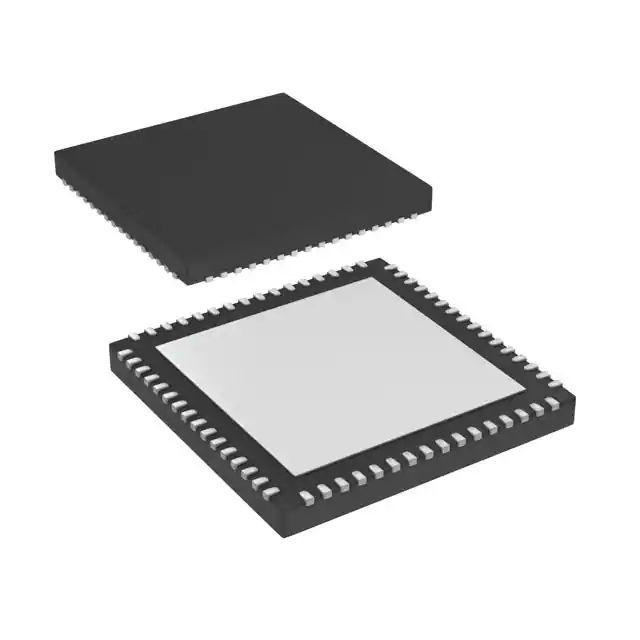
- Part No.:
- ATMEGA256RFR2-ZU
- Manufacturer:
- Microchip Technology
- Category:
- RF Transceiver ICs
- Package:
- 64-VFQFN Exposed Pad
- Datasheet:
-
 ATMEGA256RFR2-ZU.pdf
- Description:
- IC RF TXRX+MCU 802.15.4 64QFN
- Quantity:
- Payment:

- Shipping:

Inventory:155
Please send an inquiry. Send us your inquiry, and we will respond immediately.
Product details
Overview
ATMEGA256RFR2-ZU from Microchip Technology (formerly Atmel) is an 8-bit AVR microcontroller with integrated 2.4 GHz IEEE 802.15.4/ZigBee transceiver in a 64-pin QFN package. It delivers 256 KB Flash, 32 KB SRAM, 8 KB EEPROM, -100 dBm RX sensitivity, and 3.5 dBm TX output power. It operates from 1.8–3.6 V and supports 250 kb/s to 2 Mb/s data rates for low-power wireless sensor networks.
For engineers reviewing the ATMEGA256RFR2-ZU datasheet, ATMEGA256RFR2-ZU pinout, ATMEGA256RFR2-ZU application, or ATMEGA256RFR2-ZU equivalent, key selection criteria include integrated MAC hardware acceleration, AES-128 security engine, 38 programmable I/O lines, deep-sleep current <700 nA, and dual crystal support (16 MHz + 32.768 kHz).
Technical Context
The ATMEGA256RFR2-ZU integrates an enhanced RISC CPU with 135 single-cycle instructions and a fully integrated 2.4 GHz DSSS transceiver featuring hardware-assisted MAC, auto-acknowledge, auto-retry, and 32-bit IEEE 802.15.4 symbol counter. Its fractional-N PLL provides 5 MHz/500 kHz channel spacing.
It combines AVDD/DVDD internal regulators, dedicated RF ground pins (AVSS_RFP/AVSS_RFN), differential RF I/O (RFP/RFN), and hardware AES encryption with true random number generation - all within a single die optimized for ZigBee Pro coordinator/router applications requiring robust coexistence and ultra-low power operation.
Key Specifications
| Parameter | Value and Actual Design Meaning |
|---|---|
| Core Architecture | AVR 8-bit RISC with 32 general-purpose registers and 2-cycle hardware multiplier |
| Flash Memory | 256 KB ISP Flash with read-while-write capability for firmware updates without halting execution |
| Transceiver Data Rates | 250 kb/s, 500 kb/s, 1 Mb/s, and 2 Mb/s - selectable per link budget and interference environment |
| RX Sensitivity | -100 dBm at 250 kb/s - enables reliable reception at extended range in noisy ISM band environments |
| TX Output Power | Up to +3.5 dBm - sufficient for mesh routing without external PA in most indoor deployments |
| Supply Current (Deep Sleep) | <700 nA @ 25°C - supports multi-year battery life in wake-on-RF or timer-triggered sensor nodes |
| Operating Voltage | 1.8–3.6 V - compatible with coin cells (e.g., CR2032) and Li-ion/Li-Po battery systems |
| Temperature Range | -40°C to +125°C - qualified for industrial and harsh-environment embedded deployment |
Pinout & Package
ATMEGA256RFR2-ZU uses a 64-pad QFN (RoHS/Fully Green) package with exposed metal paddle internally connected to AVSS. The paddle must be soldered to PCB ground for mechanical stability and thermal performance; leaving it unconnected risks package detachment.
| Pin/Terminal | Circuit Role | Design Meaning |
|---|---|---|
| RFP / RFN | Differential RF I/O | 100 Ω differential port requiring balun for 50 Ω single-ended antenna interface; supports antenna diversity control |
| AVSS_RFP / AVSS_RFN | Dedicated RF Ground | Separate analog ground returns for RF section to minimize coupling into digital domains |
| XTAL1 / XTAL2 | 16 MHz Crystal Interface | Drives transceiver PLL; requires low-parasitic layout and 12 pF load capacitors for stable 2.4 GHz synthesis |
| TST / CLKI | Test & Clock Input | TST enables programming mode; CLKI allows external clock injection - both must be externally terminated |
| DEVDD / EVDD | Digital & Analog Supplies | External 1.8–3.6 V inputs feeding internal DVDD/AVDD regulators - bypassing critical for noise immunity |
| PG0–PG5, PB0–PB7, PD0–PD7, PE0–PE7, PF0–PF7 | Programmable I/O | 38 total GPIO with alternate functions including USART, SPI, TWI, ADC, timers, and RF indicators (DIG1–DIG4) |
Key Features
| Feature | Design Value |
|---|---|
| Hardware MAC Acceleration | Offloads frame filtering, CRC-16, SFD detection, and auto-ACK/retry - reduces CPU load and latency in dense networks |
| AES-128 Security Engine | Dedicated cryptographic accelerator with true random number generator - enables secure key exchange and payload encryption without software overhead |
| Dual Crystal Oscillators | 16 MHz for transceiver timing and 32.768 kHz for low-power RTC/MAC symbol counter - eliminates need for external real-time clock IC |
| Phase Measurement Support | Enables time-of-flight (ToF) and angle-of-arrival (AoA) calculations for precise indoor localization applications |
| Antenna Diversity Control | Hardware-switched RF path selection via DIG1/DIG2 pins - improves link reliability in multipath environments |
| Ultra-Low Deep-Sleep Current | <700 nA with 32.768 kHz oscillator and MAC symbol counter active - extends battery life beyond 10 years in periodic wake-up sensors |
Applications
| ZigBee Pro Coordinator | Industrial Wireless Sensor Node |
|---|---|
Use Scenario: Central network manager in smart building automation, aggregating data from hundreds of end devices and routing traffic across multiple PANs. IC Role / Device Role / Timing Role: Full-function ZigBee Pro coordinator with hardware-accelerated MAC, AES security, and 32-bit symbol counter for precise timestamping and synchronization. Use Value: 256 KB Flash stores full ZigBee stack + application logic; -100 dBm sensitivity ensures reliable uplink from distant sensors; deep-sleep current enables always-on operation on backup power. | Use Scenario: Battery-powered temperature/humidity/pressure sensor deployed in factory floors or HVAC ducts with 5+ year maintenance intervals. IC Role / Device Role / Timing Role: Self-contained sensor node with integrated ADC, RF transceiver, and ultra-low-power sleep modes - wakes only on timer or interrupt to transmit encrypted readings. Use Value: On-chip 32.768 kHz oscillator maintains accurate timekeeping during sleep; hardware AES encrypts payloads before transmission; <700 nA deep-sleep current enables decade-long battery life. |
| 6LoWPAN Border Router | WirelessHART Field Device |
Use Scenario: IPv6 gateway bridging IEEE 802.15.4 mesh networks to Ethernet/Wi-Fi infrastructure in IIoT deployments. IC Role / Device Role / Timing Role: Dual-role device running 6LoWPAN adaptation layer and UDP/IP stack while managing neighbor discovery and route optimization. Use Value: 32 KB SRAM accommodates IPv6 header compression buffers and socket tables; hardware MAC offload preserves CPU cycles for protocol processing; 2 Mb/s mode accelerates bulk configuration updates. | Use Scenario: Loop-powered field instrument in hazardous process plants requiring intrinsic safety compliance and deterministic latency. IC Role / Device Role / Timing Role: WirelessHART-compliant device implementing TDMA scheduling, channel hopping, and redundant transmission using hardware symbol counter and frame buffering. Use Value: Hardware-assisted frame handling ensures sub-100 ms jitter for closed-loop control; TX/RX 128-byte buffers absorb burst traffic; phase measurement supports synchronized sampling across distributed nodes. |
Equivalent & Alternatives
The following parts are listed as comparable options for similar 8-bit wireless microcontroller applications.
| Alternative Part | Technical Difference | Application Difference | Selection Advice |
|---|---|---|---|
| ATMEGA128RFR2-ZU | 128 KB Flash, 16 KB SRAM, 4 KB EEPROM - reduced memory footprint and lower static current | Targeted for ZigBee routers or mid-tier coordinators with smaller stack requirements | Select when full ZigBee Pro stack size exceeds 128 KB or when >32 KB RAM is needed for large routing tables |
| CC2652R1F | ARM Cortex-M4F core, 352 KB Flash, 80 KB RAM, Bluetooth 5.1 + IEEE 802.15.4 dual-mode radio | Supports BLE mesh, Thread, and ZigBee simultaneously; higher compute throughput but larger code size | Select when multi-protocol interoperability, advanced signal processing, or future-proofing beyond ZigBee is required |
Compared with ATMEGA128RFR2-ZU, the ATMEGA256RFR2-ZU provides double Flash/SRAM for complex coordinator stacks and larger routing tables; compared with CC2652R1F, it offers lower power in pure ZigBee deployments and simpler toolchain integration for legacy AVR-based designs.
Availability
ATMEGA256RFR2-ZU is available at Aetrix Electronics and suitable for industrial wireless sensor networks, smart building automation systems, and IIoT edge gateways requiring stable component supply, long-term lifecycle assurance, and RoHS-compliant packaging.
Supply support for ATMEGA256RFR2-ZU includes scheduled delivery planning, volume procurement assistance, BOM continuity management, traceable sourcing, and lifecycle availability coordination for OEM customers, industrial embedded developers, connected-device designers, and electronics production programs.
Manufacturer
Microchip Technology acquired Atmel in 2016 and continues to develop, manufacture, and support the AVR microcontroller portfolio with focus on robustness, longevity, and embedded design simplicity.
The ATMEGA256RFR2-ZU belongs to the AVR Wireless family designed specifically for standards-compliant, ultra-low-power IEEE 802.15.4 and ZigBee Pro applications - emphasizing integrated RF, hardware security, and minimal external component count.
FAQ
What is the maximum TX output power of the ATMEGA256RFR2-ZU and how is it configured?
The ATMEGA256RFR2-ZU delivers up to +3.5 dBm TX output power in its highest setting. This value is achieved through internal PA biasing controlled by register bits in the RF_CTRL register. Power levels can be reduced in discrete steps (e.g., +1.5 dBm, -1 dBm, -5 dBm) to optimize range versus battery life. The ATMEGA256RFR2-ZU does not require external matching components beyond the balun and DC-blocking capacitors specified in the reference schematic.
Does the ATMEGA256RFR2-ZU support over-the-air (OTA) firmware updates?
Yes, the ATMEGA256RFR2-ZU supports OTA firmware updates via its integrated 2.4 GHz transceiver and ISP Flash architecture. The bootloader resides in protected boot Flash space and can receive encrypted application images over ZigBee or custom 802.15.4 frames. Because the ATMEGA256RFR2-ZU implements true Read-While-Write Flash, application code continues executing during reprogramming - enabling seamless, non-disruptive updates in live networks.
How many ADC channels does the ATMEGA256RFR2-ZU have and what is their resolution?
The ATMEGA256RFR2-ZU features an 8-channel, 10-bit successive-approximation ADC with differential input capability and programmable gain. Channels are mapped to Port F pins PF0–PF7. It achieves 330 ks/s sampling rate and includes an on-chip temperature sensor. The ADC supports free-running, single-conversion, and event-triggered modes - all configurable via the ADC multiplexer and control registers in the ATMEGA256RFR2-ZU datasheet.
Is the ATMEGA256RFR2-ZU pin-compatible with the ATMEGA2561 or ATMEGA1281?
The ATMEGA256RFR2-ZU shares register-level compatibility with ATMEGA2561/1281 for most peripherals but is not pin-compatible. Ports A and C are omitted; RF-specific pins (RFP, RFN, AVSS_RFP, AVSS_RFN) replace former address/data bus functions. TST replaces BS2 for programming entry. While software migration is feasible with minor register mapping adjustments, PCB layout requires redesign due to the 64-pin QFN RF-optimized pinout and dedicated ground structure of the ATMEGA256RFR2-ZU.
What crystal frequencies are required for the ATMEGA256RFR2-ZU and why are two needed?
The ATMEGA256RFR2-ZU requires two crystals: a 16 MHz fundamental-mode crystal on XTAL1/XTAL2 for the transceiver's PLL and RF timing, and a 32.768 kHz tuning-fork crystal on PG3/PG4 for the asynchronous timer and IEEE 802.15.4 symbol counter. The 16 MHz crystal ensures precise 2.4 GHz carrier synthesis; the 32.768 kHz crystal enables ultra-low-power timekeeping during deep-sleep modes where the main oscillator is disabled - both are mandatory for full ZigBee Pro compliance and low-energy operation.
ATMEGA256RFR2-ZU Specifications
- Product attributes
- Attribute value
- Manufacturer:
- Microchip Technology
- Series:
- -
- Package/Case:
- 64-VFQFN Exposed Pad
- Packaging:
- Tray
- Product Status:
- Active
- Programmable:
- Not Verified
- Type:
- TxRx + MCU
- RF Family/Standard:
- 802.15.4
- Protocol:
- Zigbee®
- Modulation:
- DSSS, O-QPSK
- Frequency:
- 2.4GHz
- Data Rate (Max):
- 2Mbps
- Power - Output:
- 3.5dBm
- Sensitivity:
- -100dBm
- Memory Size:
- 256kB Flash, 8kB EEPROM, 32kB SRAM
- Serial Interfaces:
- I2C, JTAG, SPI, USART
- GPIO:
- 35
- Voltage - Supply:
- 1.8V ~ 3.6V
- Current - Receiving:
- 5mA ~ 12.5mA
- Current - Transmitting:
- 8mA ~ 14.5mA
- Operating Temperature:
- -40°C ~ 85°C
- Grade:
- -
- Qualification:
- -
- Supplier Device Package:
- 64-QFN (9x9)
ATMEGA256RFR2-ZU FAQ
1.How can I place an order for ATMEGA256RFR2-ZU through Aetrix?
Please submit a Request for Quotation (RFQ) for ATMEGA256RFR2-ZU on Aetrix. Our sales agent will provide a competitive quotation and guide you through the order confirmation once you accept the terms.
2.Are the price and stock information for ATMEGA256RFR2-ZU reliable?
The price and inventory of ATMEGA256RFR2-ZU are updated periodically and may fluctuate due to market conditions. Stock and pricing data are typically refreshed every 24 hours. Quotation validity for ATMEGA256RFR2-ZU is usually 5 days.
3.What payment methods are accepted for ATMEGA256RFR2-ZU?
We accept Wire Transfer, PayPal, Credit Card, Western Union, MoneyGram, and Escrow for ATMEGA256RFR2-ZU transactions.
Note: Certain payment methods may incur a processing fee.
4.How is shipping managed for ATMEGA256RFR2-ZU?
ATMEGA256RFR2-ZU orders can be shipped via leading logistics carriers, including DHL, UPS, FedEx, TNT, or Registered Mail.
Once your ATMEGA256RFR2-ZU order is processed, you will receive an email with the shipment details and tracking number.
Note: Tracking information may take up to 24 hours to appear. Express delivery typically takes 3–5 business days.
5.How can I obtain technical support or documentation for ATMEGA256RFR2-ZU?
For technical support, including ATMEGA256RFR2-ZU datasheets, pinout diagrams, or application guidance, please contact our engineering support team. They can provide detailed documentation and assistance for your ATMEGA256RFR2-ZU requirements.
6.How does Aetrix verify that ATMEGA256RFR2-ZU is sourced from the original manufacturer or authorized distributors?
All ATMEGA256RFR2-ZU products on Aetrix are procured from qualified distributors and authorized channels. Our dedicated quality assurance team conducts strict verification, including traceability checks and, if necessary, third-party testing. This ensures that ATMEGA256RFR2-ZU meets industry standards.
7.What is the process for return or replacement of ATMEGA256RFR2-ZU?
All ATMEGA256RFR2-ZU units undergo pre-shipment inspection (PSI). If there is an issue with ATMEGA256RFR2-ZU, returns or replacements are accepted under the following conditions:
1.Quantity discrepancies, incorrect items, or visible external defects (such as breakage or corrosion), acknowledged by Aetrix.
2.The issue is reported within 90 days of delivery.
3.The ATMEGA256RFR2-ZU part is unused and in its original packaging.
Return procedure for ATMEGA256RFR2-ZU:
1.Submit a request within 90 days.
2.Obtain a Return Material Authorization (RMA) from Aetrix.
ATMEGA256RFR2-ZU Tags

-
ESP32-D0WD-V3
Espressif Systems

-
ESP8266EX
Espressif Systems

-
ESP32-S3
Espressif Systems

-
NRF24L01P-R7
Nordic Semiconductor ASA
-
NRF24L01P-R
Nordic Semiconductor ASA

-
ESP32-U4WDH
Espressif Systems

-
DA14531-00000OG2
Renesas
-
ESP32-C6FH4
Espressif Systems

-
DA14531-00000FX2
Renesas
-
NRF24L01P-T
Nordic Semiconductor ASA

-
NRF52810-QCAA-R
Nordic Semiconductor ASA
-
ESP32-S3FN8
Espressif Systems
Tech Hub

TTL and CMOS logic families differ in thresholds, loading, output drive, power and timing. This engineering guide compares 74HC and 74HCT, calculates noise margins and checks 3.3 V/5 V compatibility.

A practical engineering guide to 3.3V and 5V logic compatibility, input thresholds, resistor dividers, translator ICs, MOSFET level shifting, I2C pull-ups, timing limits and power-sequencing risks.

The 74HC595 uses push-pull logic outputs, while the TPIC6B595 uses 50 V open-drain DMOS sinks for higher-power loads. This guide compares timing, current limits, 3.3 V interfacing, load wiring, thermal…

The 74HC595 converts serial data into eight stable parallel outputs. This guide covers pin functions, shift and storage timing, OE and MR behavior, drive-current limits, cascading, voltage compatibilit…

A technical comparison of level-sensitive latches and edge-triggered flip-flops, covering timing windows, setup and hold limits, master–slave operation, time borrowing, race-through, HDL inference and…

A D latch stores one bit while Enable controls when data can pass. This reference covers gate-level operation, truth tables, transparency, setup and hold timing, LE versus OE, common ICs and practical …

An SR latch stores one bit through cross-coupled feedback. This engineering reference covers NOR and NAND implementations, truth tables, forbidden-state recovery, gated operation, switch debouncing, fa…

Latch circuits retain one bit through feedback. This technical reference covers SR and D latches, truth tables, transparency, timing limits, latch-versus-flip-flop behavior, applications and common log…

An engineering guide to LED driver operation, constant-current and constant-voltage outputs, linear and switching topologies, dimming, IC selection, calculations, replacement compatibility, and fault c…

Operational amplifier guide covering op amp basics, feedback, ideal vs real op amps, common configurations, buffer circuits, offset, bias current, gain-bandwidth, slew rate, rail-to-rail limits and sel…


