
 My Inquiry
 My Account


Skyworks Solutions Inc. ATN3580-30
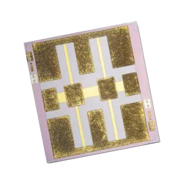
- Part No.:
- ATN3580-30
- Manufacturer:
- Skyworks Solutions Inc.
- Category:
- Attenuators
- Package:
- Module
- Datasheet:
-
 ATN3580-30.pdf
- Description:
- RF ATTENUATOR 30DB MODULE
- Quantity:
- Payment:

- Shipping:

Inventory:4,722
Please send an inquiry. Send us your inquiry, and we will respond immediately.
Product details
Overview
ATN3580-30 from Skyworks Solutions is a fixed thin-film silicon attenuator chip delivering 30 dB nominal attenuation with ±1.60 dB DC tolerance, ±0.5 dB flatness from 0.1–7 GHz, and minimum 15 dB return loss up to 40 GHz. It uses a balanced TEE resistive structure, handles 1 W CW incident power, and operates from –55 °C to +150 °C in RF signal conditioning paths for test instrumentation and microwave transceivers.
For engineers reviewing the ATN3580-30 datasheet, ATN3580-30 pinout, ATN3580-30 application, or ATN3580-30 equivalent, key selection criteria include broadband flatness stability, high-power handling at elevated temperature, RoHS-compliant rugged die construction, and compatibility with standard ribbon-bond or flip-chip mounting per 518-060 outline.
Technical Context
The ATN3580-30 implements a balanced TEE topology using precision thin-film resistors on high-resistivity silicon, enabling stable 30 dB attenuation across DC–40 GHz. Its design achieves ≥15 dB return loss up to 40 GHz and maintains ±2.0 dB flatness over the full 0.1–40 GHz band.
It is rated for 1 W CW incident power at 25 °C with absolute maximum operating temperature of +150 °C and storage range from –65 °C to +150 °C. ESD robustness includes 1000 V CDM, 2000 V HBM, and 200 V MM ratings.
Key Specifications
| Parameter | Value and Actual Design Meaning |
|---|---|
| Nominal attenuation | 30 dB ±1.60 dB at DC - defines insertion loss baseline for RF path calibration |
| Attenuation flatness (0.1–40 GHz) | ±2.0 dB - ensures consistent signal reduction across Ka-band and millimeter-wave applications |
| Minimum return loss (0.1–40 GHz) | 15 dB - reduces VSWR-induced measurement uncertainty in 50 Ω systems |
| Power handling | 1 W CW at 25 °C - supports continuous operation in high-level RF test fixtures |
| Operating temperature | –55 °C to +150 °C - enables deployment in aerospace, defense, and under-hood automotive RF modules |
| Package outline | 518-060 - 0.060 × 0.060 inch ceramic chip with defined land pattern for ribbon bonding |
Pinout & Package
ATN3580-30 is a two-terminal passive chip device in a 518-060 outline (0.060 × 0.060 inch), with no internal pins or active circuitry. It features RF input and RF output terminals defined by metallized pads on opposite edges of the die, intended for wire-bond or ribbon-attach interconnection in 50 Ω microstrip environments.
| Pin/Terminal | Circuit Role | Design Meaning |
|---|---|---|
| Terminal 1 | RF Input | Primary signal entry point; requires impedance-matched feedline to minimize reflection |
| Terminal 2 | RF Output | Attenuated signal exit; designed for direct connection to downstream mixer or amplifier input |
Key Features
| Feature | Design Value |
|---|---|
| Balanced TEE resistive architecture | Enables broadband flatness and symmetrical port matching without external bias or control lines |
| Thin-film silicon construction | Delivers higher power density and thermal stability than thick-film alternatives, supporting 1 W CW |
| DC–40 GHz bandwidth | Validated performance up to Ka-band frequencies, suitable for 5G FR2 and satellite comms front-ends |
| Ruggedized die packaging | RoHS-compliant, Pb-free Green™ construction with CDM/HBM/MM ESD protection for assembly reliability |
Applications
| Test & Measurement Instrumentation | Millimeter-Wave Transceiver Front-Ends |
|---|---|
Use Scenario: Signal level adjustment in vector network analyzer (VNA) calibration kits and RF power sensor reference paths. IC Role / Device Role / Timing Role: Passive fixed attenuator providing traceable 30 dB loss for amplitude accuracy verification. Use Value: ±2.0 dB flatness over 0.1–40 GHz ensures calibrated loss remains within specification across full instrument bandwidth. | Use Scenario: Inter-stage isolation and gain control in Ka-band phased-array radar transmit/receive modules. IC Role / Device Role / Timing Role: Two-terminal RF attenuator placed between PA driver and power amplifier to suppress harmonic coupling. Use Value: 15 dB return loss minimizes reflected energy that could destabilize wideband GaN PAs operating near 30 GHz. |
| 5G NR FR2 Base Station Radios | Aerospace & Defense EW Systems |
Use Scenario: Input protection and dynamic range management for mmWave beamformer ICs in massive MIMO active antennas. IC Role / Device Role / Timing Role: Fixed-loss element in RF chain prior to ADC input to prevent saturation during high-SNR bursts. Use Value: Stable 30 dB attenuation at +105 °C ambient enables reliable operation in sealed outdoor radio enclosures. | Use Scenario: Signal conditioning in electronic warfare receiver front-ends requiring wideband, high-reliability attenuation. IC Role / Device Role / Timing Role: Hermetically mountable passive attenuator used in channelized receiver IF strips for threat signal simulation. Use Value: –55 °C to +150 °C operating range and 1000 V CDM rating support survivability in harsh airborne and missile platform environments. |
Equivalent & Alternatives
The following parts are listed as comparable options for similar fixed attenuator applications.
| Alternative Part | Technical Difference | Application Difference | Selection Advice |
|---|---|---|---|
| Mini-Circuits VAT-30W2+ | Surface-mount ceramic package; 30 dB ±0.5 dB (0.1–26.5 GHz); 2 W power rating; larger 0.125 × 0.062 inch footprint | Designed for PCB-level integration with solder reflow; less suited for hybrid microcircuit or ribbon-bond assemblies | Select when board space allows larger footprint and higher power margin is required beyond 1 W |
| Qorvo QPA1003 | Active GaAs MMIC attenuator; 30 dB programmable via analog voltage; 0.1–40 GHz; 0.5 W max; requires bias and control lines | Used where variable attenuation or remote control is needed; adds complexity versus passive solution | Select only if dynamic adjustment capability justifies added design overhead and power supply requirements |
Compared with VAT-30W2+ and QPA1003, the ATN3580-30 offers superior broadband flatness stability in hybrid assemblies, eliminates bias/control circuitry, and fits compact 518-060 land patterns-making it optimal for high-density RF modules where simplicity, size, and temperature resilience are critical.
Availability
ATN3580-30 is available at Aetrix Electronics and suitable for RF test equipment, millimeter-wave communications infrastructure, and aerospace EW subsystems requiring stable component supply across extended temperature and frequency ranges.
Supply support for ATN3580-30 includes scheduled delivery planning, volume procurement assistance, BOM continuity management, traceable sourcing, and lifecycle availability coordination for OEM customers, industrial embedded developers, connected-device designers, and electronics production programs.
Manufacturer
Skyworks Solutions is a global semiconductor company specializing in analog and mixed-signal connectivity solutions for wireless, broadband, automotive, and industrial markets.
The ATN3580 series belongs to Skyworks' high-frequency passive components product line, engineered specifically for broadband RF signal conditioning in test, defense, and 5G infrastructure applications where precision, ruggedness, and wideband flatness are essential.
FAQ
What is the DC attenuation tolerance for ATN3580-30?
The ATN3580-30 has a nominal attenuation of 30 dB with a DC tolerance of ±1.60 dB, as specified in Table 2 of the Skyworks datasheet. This tolerance applies at DC and forms the baseline for all frequency-dependent flatness specifications. The ATN3580-30 maintains this precision across its operating temperature range without drift compensation circuitry.
Does ATN3580-30 require DC bias or control signals?
No, the ATN3580-30 is a fully passive thin-film attenuator chip with no active circuitry, bias inputs, or control interfaces. It functions solely as a two-terminal RF component and requires no power supply, ground reference, or digital/analog control lines. The ATN3580-30 operates identically whether DC-coupled or AC-coupled in the signal path.
What is the recommended mounting method for ATN3580-30?
Skyworks specifies ribbon bonding or flip-chip attachment for the ATN3580-30 per Figures 4 and 5 in the datasheet, aligned with the 518-060 outline. Die mounting should follow the suggested land pattern in Figure 7, using conductive epoxy or eutectic solder compatible with gold metallization. Wire bonding is not recommended due to mechanical stress on the thin-film structure.
Can ATN3580-30 be used above 40 GHz?
No-performance is only guaranteed up to 40 GHz per datasheet specifications. While some insertion loss and return loss data may extend beyond 40 GHz in typical curves, Skyworks does not characterize or warrant operation above 40 GHz for the ATN3580-30. For >40 GHz applications, alternative solutions such as waveguide or MMIC-based attenuators should be evaluated.
Is ATN3580-30 compliant with RoHS and lead-free requirements?
Yes, the ATN3580-30 is lead (Pb)-free, RoHS-compliant, and certified as Skyworks Green™ per the Skyworks Certificate of Conformance. Its metallization and substrate materials meet EU Directive 2011/65/EU and subsequent amendments, with full traceability documentation available upon request for the ATN3580-30.
ATN3580-30 Specifications
- Product attributes
- Attribute value
- Manufacturer:
- Skyworks Solutions Inc.
- Package/Case:
- Module
- Series:
- ATN3580
- Packaging:
- Tray
- Product Status:
- Active
- Attenuation Value:
- 30dB
- Frequency Range:
- 100 MHz ~ 40 GHz
- Power (Watts):
- 1W
- Impedance:
- -
- Grade:
- -
- Qualification:
- -
ATN3580-30 FAQ
1.How can I place an order for ATN3580-30 through Aetrix?
Please submit a Request for Quotation (RFQ) for ATN3580-30 on Aetrix. Our sales agent will provide a competitive quotation and guide you through the order confirmation once you accept the terms.
2.Are the price and stock information for ATN3580-30 reliable?
The price and inventory of ATN3580-30 are updated periodically and may fluctuate due to market conditions. Stock and pricing data are typically refreshed every 24 hours. Quotation validity for ATN3580-30 is usually 5 days.
3.What payment methods are accepted for ATN3580-30?
We accept Wire Transfer, PayPal, Credit Card, Western Union, MoneyGram, and Escrow for ATN3580-30 transactions.
Note: Certain payment methods may incur a processing fee.
4.How is shipping managed for ATN3580-30?
ATN3580-30 orders can be shipped via leading logistics carriers, including DHL, UPS, FedEx, TNT, or Registered Mail.
Once your ATN3580-30 order is processed, you will receive an email with the shipment details and tracking number.
Note: Tracking information may take up to 24 hours to appear. Express delivery typically takes 3–5 business days.
5.How can I obtain technical support or documentation for ATN3580-30?
For technical support, including ATN3580-30 datasheets, pinout diagrams, or application guidance, please contact our engineering support team. They can provide detailed documentation and assistance for your ATN3580-30 requirements.
6.How does Aetrix verify that ATN3580-30 is sourced from the original manufacturer or authorized distributors?
All ATN3580-30 products on Aetrix are procured from qualified distributors and authorized channels. Our dedicated quality assurance team conducts strict verification, including traceability checks and, if necessary, third-party testing. This ensures that ATN3580-30 meets industry standards.
7.What is the process for return or replacement of ATN3580-30?
All ATN3580-30 units undergo pre-shipment inspection (PSI). If there is an issue with ATN3580-30, returns or replacements are accepted under the following conditions:
1.Quantity discrepancies, incorrect items, or visible external defects (such as breakage or corrosion), acknowledged by Aetrix.
2.The issue is reported within 90 days of delivery.
3.The ATN3580-30 part is unused and in its original packaging.
Return procedure for ATN3580-30:
1.Submit a request within 90 days.
2.Obtain a Return Material Authorization (RMA) from Aetrix.
ATN3580-30 Tags

-
PAT0510S-C-3DB-T10
Susumu
-
PAT0510S-C-10DB-T10
Susumu
-
PAT0510S-C-2DB-T10
Susumu
-
PAT1220-C-10DB-T5
Susumu
-
PAT1220-C-6DB-T5
Susumu
-
PAT1220-C-0DB-T5
Susumu
-
PAT1220-C-3DB-T5
Susumu
-
PAT1220-C-5DB-T5
Susumu
-
PAT1220-C-8DB-T5
Susumu
-
MAADSS0008TR-3000
MACOM Technology Solutions
-
MAATSS0018TR-3000
MACOM Technology Solutions
-
PE43205B-Z
pSemi
Tech Hub

Counterfeit components can hide behind convincing markings and passing basic function tests. This engineering reference covers source traceability, external inspection, X-ray, XRF, electrical testing, …

A practical engineering and sourcing framework covering lifecycle verification, lifetime-buy calculations, replacement qualification, supplier checks and counterfeit-risk controls.

TTL and CMOS logic families differ in thresholds, loading, output drive, power and timing. This engineering guide compares 74HC and 74HCT, calculates noise margins and checks 3.3 V/5 V compatibility.

A practical engineering guide to 3.3V and 5V logic compatibility, input thresholds, resistor dividers, translator ICs, MOSFET level shifting, I2C pull-ups, timing limits and power-sequencing risks.

The 74HC595 uses push-pull logic outputs, while the TPIC6B595 uses 50 V open-drain DMOS sinks for higher-power loads. This guide compares timing, current limits, 3.3 V interfacing, load wiring, thermal…

The 74HC595 converts serial data into eight stable parallel outputs. This guide covers pin functions, shift and storage timing, OE and MR behavior, drive-current limits, cascading, voltage compatibilit…

A technical comparison of level-sensitive latches and edge-triggered flip-flops, covering timing windows, setup and hold limits, master–slave operation, time borrowing, race-through, HDL inference and…

A D latch stores one bit while Enable controls when data can pass. This reference covers gate-level operation, truth tables, transparency, setup and hold timing, LE versus OE, common ICs and practical …

An SR latch stores one bit through cross-coupled feedback. This engineering reference covers NOR and NAND implementations, truth tables, forbidden-state recovery, gated operation, switch debouncing, fa…

Latch circuits retain one bit through feedback. This technical reference covers SR and D latches, truth tables, transparency, timing limits, latch-versus-flip-flop behavior, applications and common log…


