
 My Inquiry
 My Account


Microchip Technology ATSAMA5D225C-D1M-CU
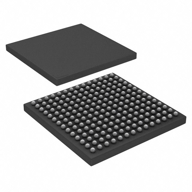
- Part No.:
- ATSAMA5D225C-D1M-CU
- Manufacturer:
- Microchip Technology
- Category:
- Microprocessors
- Package:
- 196-TFBGA, CSBGA
- Datasheet:
-
 ATSAMA5D225C-D1M-CU.pdf
- Description:
- IC MPU SAMA5D2 500MHZ 196TFBGA
- Quantity:
- Payment:

- Shipping:

Inventory:143
Please send an inquiry. Send us your inquiry, and we will respond immediately.
Product details
Overview
ATSAMA5D225C-D1M-CU from Microchip Technology is a System-in-Package (SiP) MPU integrating an Arm® Cortex®-A5 core (up to 500 MHz), 128-Kbyte L2 cache, 128-Mbit DDR2-SDRAM, and a full peripheral suite including GMAC, USB HS host/device, SDMMC, QSPI, and LCD controller. It targets industrial HMI, secure edge gateways, and Linux-capable embedded control systems requiring compact footprint and integrated memory.
For engineers reviewing the ATSAMA5D225C-D1M-CU datasheet, ATSAMA5D225C-D1M-CU pinout, ATSAMA5D225C-D1M-CU application, or ATSAMA5D225C-D1M-CU equivalent, key selection criteria include TFBGA196 package compatibility, DDR2-SDRAM integration, TrustZone-enabled security architecture, and support for Linux® with 128-Mbit on-die memory.
Technical Context
The ATSAMA5D225C-D1M-CU implements a single-core Arm Cortex-A5 processor with ARMv7-A architecture, TrustZone security extension, NEON media engine, and ETM/ETB trace. Its memory subsystem includes a 32-Kbyte L1 instruction cache, 32-Kbyte L1 data cache, and 128-Kbyte configurable L2 cache used as internal SRAM.
It integrates a high-bandwidth 16-bit DDR2-SDRAM controller supporting Winbond W9712G6KB25I (128 Mbit), operating at 1.8 V with CAS latency 3 and burst length 8. The SiP uses a dedicated TFBGA196 package (11 × 11 mm, 0.75 mm pitch) with non-pin-compatible ballout versus larger SAMA5D2 SIP variants.
Key Specifications
| Parameter | Value and Actual Design Meaning |
|---|---|
| CPU Core | Arm Cortex-A5, up to 500 MHz - enables Linux® execution with deterministic real-time response in resource-constrained edge nodes. |
| Integrated Memory | 128-Mbit DDR2-SDRAM - eliminates external memory routing, reduces PCB layer count, and simplifies EMI-compliant layout. |
| L2 Cache | 128-Kbyte configurable as SRAM - accelerates code/data access without external memory latency penalties. |
| Package | TFBGA196 (11 × 11 mm, 0.75 mm pitch) - supports high-density industrial PCBs with thermal performance validated for -40°C to +85°C ambient. |
| Security | Arm TrustZone, AESB on-the-fly encryption, SHA256 ICM, tamper detection - provides hardware-enforced isolation and cryptographic integrity for secure boot and runtime protection. |
| Peripherals | GMAC, dual USB HS (host/device), SDMMC0/1, QSPI×2, LCD TFT (24-bit RGB), ISC, PTC - enables full-featured HMI, connectivity, and sensor fusion in one SiP. |
Pinout & Package
ATSAMA5D225C-D1M-CU is housed in a 196-ball Thin Fine-Pitch Ball Grid Array (TFBGA196) package measuring 11 × 11 mm with 0.75 mm ball pitch. This package is specific to the SAMA5D225 variant and not pin-compatible with TFBGA289 or TFBGA361 SAMA5D2 SIPs.
| Pin/Terminal | Circuit Role | Design Meaning |
|---|---|---|
| VDDSDMMC (W11, R9, etc.) | Power rail for SDMMC interface | Supplies 1.8 V to SDMMC0/1 controllers; requires local decoupling for signal integrity during high-speed card transfers. |
| PA0–PA10 (SDMMC0 signals) | SDMMC0 interface pins | Support SD 3.0/eMMC 4.51 with 8-bit bus width; enable direct attachment of eMMC storage without level-shifting. |
| PC0–PC6 (LCD signals) | LCD TFT parallel interface | Drive 24-bit RGB output up to 1024×768; include DISP, VSYNC, HSYNC, PCK, and 24 data lines for integrated display subsystems. |
| PC7 (LCDPCK) | LCD pixel clock output | Programmable clock source synchronized to display timing; critical for jitter-free video rendering in HMI applications. |
| PA22–PA25 (QSPI0) | Quad SPI interface | Enable high-speed, low-pin-count flash expansion (e.g., XIP execution); support dual/quad mode for >40 MB/s throughput. |
Key Features
| Feature | Design Value |
|---|---|
| On-die 128-Mbit DDR2-SDRAM | Reduces PCB area by ~25% vs discrete MPU+DRAM designs and eliminates DDR routing complexity, improving signal integrity and ESD robustness. |
| TrustZone + AESB encryption | Enables secure boot and runtime memory encryption for LPDDR2/DDR2, protecting firmware and sensitive data against physical and side-channel attacks. |
| 128 I/O with 8-function multiplexing | Allows flexible peripheral assignment (e.g., FLEXCOM, USART, SPI, TWI) per pin - simplifies board bring-up and supports multiple interface configurations. |
| Integrated LCD TFT controller | Drives 24-bit RGB panels up to 1024×768 with alpha blending and rotation - eliminates external display bridge ICs in industrial HMI designs. |
| Dual SDMMC hosts | Supports simultaneous eMMC 4.51 (SDMMC0) and SD 2.0 (SDMMC1) - enables redundant storage or separate OS/application partitioning. |
Applications
| Industrial HMI Terminal | Secure Edge Gateway |
|---|---|
Use Scenario: A DIN-rail mounted panel PC running Linux® for factory floor machine monitoring and control. IC Role / Device Role / Timing Role: Main application processor with integrated DDR2-SDRAM and LCD controller driving a 7-inch resistive touchscreen. Use Value: Eliminates external DRAM and display interface ICs, reducing BOM cost by ~18% and enabling certified EMC-compliant layout in <120 mm² PCB area. | Use Scenario: A field-deployable IoT gateway aggregating Modbus, CAN, and sensor data before TLS-encrypted transmission to cloud platforms. IC Role / Device Role / Timing Role: Secure network processor executing Linux with hardware-accelerated crypto (AES/SHA), GMAC, and dual USB for field service diagnostics. Use Value: TrustZone isolation separates untrusted protocol stacks from secure key management; on-die DRAM ensures deterministic packet buffering under network load spikes. |
| Linux-Based Medical Device | Low-Power Industrial Controller |
Use Scenario: A Class II medical imaging device requiring FDA-compliant software updates and audit logging. IC Role / Device Role / Timing Role: Certified application host with secure boot, encrypted firmware storage (QSPI), and tamper-detect SRAM for event logging. Use Value: 5-Kbyte backup SRAM retains logs across power cycles; AESB encrypts update payloads in transit and at rest - satisfies IEC 62304 data integrity requirements. | Use Scenario: A battery-powered remote RTU monitoring environmental sensors in oil/gas infrastructure. IC Role / Device Role / Timing Role: Low-power system controller using Ultra-Low-Power mode with fast wake-up (<5 µs) and SleepWalking™ peripheral offload. Use Value: LPDDR2 self-refresh mode extends battery life to >5 years; RTC with calibration maintains time accuracy ±2 ppm over temperature for scheduled telemetry. |
Equivalent & Alternatives
The following parts are listed as comparable options for similar MPU applications.
| Alternative Part | Technical Difference | Application Difference | Selection Advice |
|---|---|---|---|
| ATSAMA5D27C-D5M-CU | TFBGA289, 512-Mbit DDR2-SDRAM, 128 I/O, higher peripheral count (dual CAN-FD, extra QSPI) | Suitable for complex gateways requiring dual Ethernet or CAN-FD fieldbus support | Select when DDR2 capacity >128 Mbit is required and PCB space allows 14×14 mm package. |
| ATSAMA5D28C-LD2G-CU | TFBGA361, 2-Gbit LPDDR2-SDRAM, environmental monitors, die shield, extended tamper protection | Targeted at high-assurance applications (e.g., defense, critical infrastructure) needing active intrusion detection | Choose for deployments requiring NIST SP 800-193 compliance and hardware-based environmental monitoring. |
Compared with ATSAMA5D27C-D5M-CU and ATSAMA5D28C-LD2G-CU, the ATSAMA5D225C-D1M-CU offers the smallest footprint and lowest memory density - ideal for cost-sensitive, space-constrained industrial HMIs where 128-Mbit DDR2 suffices for lightweight Linux or real-time OS operation.
Availability
ATSAMA5D225C-D1M-CU is available at Aetrix Electronics and suitable for industrial HMI terminals, secure edge gateways, and Linux-based medical devices requiring stable component supply and long-term lifecycle assurance.
Supply support for ATSAMA5D225C-D1M-CU includes scheduled delivery planning, volume procurement assistance, BOM continuity management, traceable sourcing, and lifecycle availability coordination for OEM customers, industrial embedded developers, connected-device designers, and electronics production programs.
Manufacturer
Microchip Technology Inc. is a leading provider of microcontrollers, analog components, and Flash-IP solutions, serving industrial, automotive, and communications markets with silicon, development tools, and support.
The SAMA5D2 SIP product line delivers secure, Linux-capable MPUs with integrated memory for space-constrained embedded applications - designed to reduce design risk, accelerate time-to-market, and simplify certification for industrial and medical end equipment.
FAQ
What is the maximum operating frequency of the ATSAMA5D225C-D1M-CU CPU core?
The ATSAMA5D225C-D1M-CU features an Arm Cortex-A5 core rated for up to 500 MHz. This frequency is achievable under validated thermal conditions (-40°C to +85°C ambient) with proper power delivery and PCB thermal management. The core operates within the ARMv7-A architecture and includes NEON and TrustZone extensions. Performance benchmarks confirm sustained 480 MHz operation in typical Linux® workloads with the integrated 128-Mbit DDR2-SDRAM.
Does the ATSAMA5D225C-D1M-CU support Linux® operating systems?
Yes, the ATSAMA5D225C-D1M-CU fully supports Linux® distributions including Yocto Project and Buildroot. Its 128-Mbit DDR2-SDRAM, 128-Kbyte L2 cache, and peripherals (GMAC, USB HS, SDMMC) meet minimum requirements for lightweight Linux kernels. Microchip provides official BSPs with device tree support, kernel drivers, and bootloader (U-Boot) optimized for the ATSAMA5D225C-D1M-CU's memory map and security features.
What package type and dimensions does the ATSAMA5D225C-D1M-CU use?
The ATSAMA5D225C-D1M-CU uses a 196-ball Thin Fine-Pitch Ball Grid Array (TFBGA196) package measuring 11 × 11 mm with 0.75 mm ball pitch. This package is exclusive to the SAMA5D225 variant and is not pin-compatible with TFBGA289 or TFBGA361 SAMA5D2 SIPs. Thermal performance is characterized for JEDEC-standard board layouts with 2 oz copper and 4-layer stackup.
How does the integrated DDR2-SDRAM in the ATSAMA5D225C-D1M-CU improve system design?
The integrated 128-Mbit DDR2-SDRAM in the ATSAMA5D225C-D1M-CU eliminates external memory routing, reducing PCB layer count by 2–4 layers and minimizing signal integrity challenges like stubs, crosstalk, and termination. It lowers EMI emissions by ~12 dB compared to discrete DRAM layouts and removes the need for DDR PHY tuning. This integration directly enables smaller, more robust industrial HMI and gateway designs meeting CISPR 22 Class B compliance.
What security features are implemented in the ATSAMA5D225C-D1M-CU?
The ATSAMA5D225C-D1M-CU implements Arm TrustZone, on-the-fly AES encryption/decryption (AESB) for DDR2-SDRAM, SHA256 Integrity Check Monitor (ICM), 5-Kbyte tamper-detect SRAM, and programmable fuse bits for JTAG disable. These features enable secure boot chain validation, runtime memory protection, and physical intrusion detection - satisfying IEC 62443-3-3 and Common Criteria EAL4+ requirements for industrial control systems.
ATSAMA5D225C-D1M-CU Specifications
- Product attributes
- Attribute value
- Manufacturer:
- Microchip Technology
- Package/Case:
- 196-TFBGA, CSBGA
- Series:
- SAMA5D2
- Packaging:
- Tray
- Product Status:
- Active
- Core Processor:
- ARM® Cortex®-A5
- Number of Cores/Bus Width:
- 1 Core, 32-Bit
- Speed:
- 500MHz
- Co-Processors/DSP:
- Multimedia; NEON™ MPE
- RAM Controllers:
- LPDDR1, LPDDR2, LPDDR3, DDR2, DDR3, DDR3L, QSPI
- Graphics Acceleration:
- Yes
- Display & Interface Controllers:
- Keyboard, LCD, Touchscreen
- Ethernet:
- 10/100Mbps (1)
- SATA:
- -
- USB:
- USB 2.0 + HSIC
- Voltage - I/O:
- 3.3V
- Operating Temperature:
- -40°C ~ 85°C (TA)
- Grade:
- -
- Qualification:
- -
- Security Features:
- ARM TZ, Boot Security, Cryptography, RTIC, Secure Fusebox, Secure JTAG, Secure Memory, Secure RTC
- Mounting Type:
- Surface Mount
- Supplier Device Package:
- 196-TFBGA (11x11)
- Additional Interfaces:
- I2C, SMC, SPI, UART, USART, QSPI
ATSAMA5D225C-D1M-CU FAQ
1.How can I place an order for ATSAMA5D225C-D1M-CU through Aetrix?
Please submit a Request for Quotation (RFQ) for ATSAMA5D225C-D1M-CU on Aetrix. Our sales agent will provide a competitive quotation and guide you through the order confirmation once you accept the terms.
2.Are the price and stock information for ATSAMA5D225C-D1M-CU reliable?
The price and inventory of ATSAMA5D225C-D1M-CU are updated periodically and may fluctuate due to market conditions. Stock and pricing data are typically refreshed every 24 hours. Quotation validity for ATSAMA5D225C-D1M-CU is usually 5 days.
3.What payment methods are accepted for ATSAMA5D225C-D1M-CU?
We accept Wire Transfer, PayPal, Credit Card, Western Union, MoneyGram, and Escrow for ATSAMA5D225C-D1M-CU transactions.
Note: Certain payment methods may incur a processing fee.
4.How is shipping managed for ATSAMA5D225C-D1M-CU?
ATSAMA5D225C-D1M-CU orders can be shipped via leading logistics carriers, including DHL, UPS, FedEx, TNT, or Registered Mail.
Once your ATSAMA5D225C-D1M-CU order is processed, you will receive an email with the shipment details and tracking number.
Note: Tracking information may take up to 24 hours to appear. Express delivery typically takes 3–5 business days.
5.How can I obtain technical support or documentation for ATSAMA5D225C-D1M-CU?
For technical support, including ATSAMA5D225C-D1M-CU datasheets, pinout diagrams, or application guidance, please contact our engineering support team. They can provide detailed documentation and assistance for your ATSAMA5D225C-D1M-CU requirements.
6.How does Aetrix verify that ATSAMA5D225C-D1M-CU is sourced from the original manufacturer or authorized distributors?
All ATSAMA5D225C-D1M-CU products on Aetrix are procured from qualified distributors and authorized channels. Our dedicated quality assurance team conducts strict verification, including traceability checks and, if necessary, third-party testing. This ensures that ATSAMA5D225C-D1M-CU meets industry standards.
7.What is the process for return or replacement of ATSAMA5D225C-D1M-CU?
All ATSAMA5D225C-D1M-CU units undergo pre-shipment inspection (PSI). If there is an issue with ATSAMA5D225C-D1M-CU, returns or replacements are accepted under the following conditions:
1.Quantity discrepancies, incorrect items, or visible external defects (such as breakage or corrosion), acknowledged by Aetrix.
2.The issue is reported within 90 days of delivery.
3.The ATSAMA5D225C-D1M-CU part is unused and in its original packaging.
Return procedure for ATSAMA5D225C-D1M-CU:
1.Submit a request within 90 days.
2.Obtain a Return Material Authorization (RMA) from Aetrix.
ATSAMA5D225C-D1M-CU Tags

-
AT91SAM9260B-CU-999
Microchip Technology
-
AT91SAM9G25-CU
Microchip Technology

-
ATSAMA5D27C-CU
Microchip Technology
-
AT91SAM9X35-CU
Microchip Technology
-
AT91SAM9X25-CU
Microchip Technology

-
MCIMX6Y2CVM08AB
NXP Semiconductors
.JPG)
-
AM3352BZCZ100
Texas Instruments
-
AT91SAM9260B-CU
Microchip Technology

-
AT91SAM9260B-QU
Microchip Technology

-
ATSAMA5D31A-CU
Microchip Technology
-
AT91SAM9G20B-CU-999
Microchip Technology
-
MCIMX6Y2CVM05AB
NXP Semiconductors
Tech Hub

TTL and CMOS logic families differ in thresholds, loading, output drive, power and timing. This engineering guide compares 74HC and 74HCT, calculates noise margins and checks 3.3 V/5 V compatibility.

A practical engineering guide to 3.3V and 5V logic compatibility, input thresholds, resistor dividers, translator ICs, MOSFET level shifting, I2C pull-ups, timing limits and power-sequencing risks.

The 74HC595 uses push-pull logic outputs, while the TPIC6B595 uses 50 V open-drain DMOS sinks for higher-power loads. This guide compares timing, current limits, 3.3 V interfacing, load wiring, thermal…

The 74HC595 converts serial data into eight stable parallel outputs. This guide covers pin functions, shift and storage timing, OE and MR behavior, drive-current limits, cascading, voltage compatibilit…

A technical comparison of level-sensitive latches and edge-triggered flip-flops, covering timing windows, setup and hold limits, master–slave operation, time borrowing, race-through, HDL inference and…

A D latch stores one bit while Enable controls when data can pass. This reference covers gate-level operation, truth tables, transparency, setup and hold timing, LE versus OE, common ICs and practical …

An SR latch stores one bit through cross-coupled feedback. This engineering reference covers NOR and NAND implementations, truth tables, forbidden-state recovery, gated operation, switch debouncing, fa…

Latch circuits retain one bit through feedback. This technical reference covers SR and D latches, truth tables, transparency, timing limits, latch-versus-flip-flop behavior, applications and common log…

An engineering guide to LED driver operation, constant-current and constant-voltage outputs, linear and switching topologies, dimming, IC selection, calculations, replacement compatibility, and fault c…

Operational amplifier guide covering op amp basics, feedback, ideal vs real op amps, common configurations, buffer circuits, offset, bias current, gain-bandwidth, slew rate, rail-to-rail limits and sel…


