
 My Inquiry
 My Account


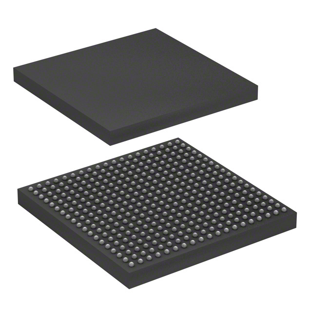
Microchip Technology ATSAMA5D27C-LD2G-CU
- Part No.:
- ATSAMA5D27C-LD2G-CU
- Manufacturer:
- Microchip Technology
- Category:
- Microprocessors
- Package:
- 361-TFBGA
- Datasheet:
-
 ATSAMA5D27C-LD2G-CU.pdf
- Description:
- IC MPU SAMA5D2 500MHZ 361TFBGA
- Quantity:
- Payment:

- Shipping:

Inventory:175
Please send an inquiry. Send us your inquiry, and we will respond immediately.
Product details
Overview
ATSAMA5D27C-LD2G-CU from Microchip Technology is a System-in-Package (SIP) MPU integrating an Arm® Cortex®-A5 core (up to 500 MHz), TrustZone® security, NEON™ media engine, and 2 Gbit LPDDR2-SDRAM in a single TFBGA361 package. It delivers high-bandwidth memory access with on-the-fly AES encryption/decryption and supports Linux®-based industrial HMI and edge gateway applications.
For engineers reviewing the ATSAMA5D27C-LD2G-CU datasheet, ATSAMA5D27C-LD2G-CU pinout, ATSAMA5D27C-LD2G-CU application, or ATSAMA5D27C-LD2G-CU equivalent, key selection considerations include LPDDR2-SDRAM integration, 128 I/Os with peripheral multiplexing, dual CAN-FD controllers, GMAC with IEEE 1588 PTP, and hardware crypto acceleration (AES-256, SHA-512, TRNG).
Technical Context
The ATSAMA5D27C-LD2G-CU implements a 32-bit Armv7-A architecture with MMU, 32-Kbyte L1 instruction/data caches, and configurable 128-Kbyte L2 cache usable as internal SRAM. Its memory subsystem features a 32-bit scramblable DDR controller supporting AP Memory LPDDR2-SDRAM up to 2 Gb at 1.8 V (VDD18) and 1.2 V (VDD12) supplies, with JEDEC LPDDR2-S4B compliance, PASR, ATCSR, and Deep Power-Down mode.
Security is enforced via Secure Boot Loader, 5 Kbytes of tamper-responsive scrambled SRAM, eight tamper pins, Integrity Check Monitor (SHA256), and hardware-accelerated cryptography including AESB for on-the-fly memory encryption. Low-power operation includes Ultra-Low-Power mode with fast wake-up and Extended Backup mode with LPDDR2 in Self-Refresh.
Key Specifications
| Parameter | Value and Actual Design Meaning |
|---|---|
| CPU Core | Arm Cortex-A5, up to 500 MHz, ARMv7-A + TrustZone® + NEON™ |
| Integrated Memory | 2 Gbit LPDDR2-SDRAM (8 Mwords × 8 Banks × 32 bits), JEDEC S4B-compliant |
| Memory Interface | 32-bit DDR multiport controller with on-the-fly AES encryption/decryption path |
| Operating Temp | -40°C to +85°C ambient, qualified for industrial environments |
| I/O Count | Up to 128 fully programmable I/Os with up to 8 peripheral functions per pin |
| Security Features | Secure Boot Loader, SHA256 ICM, AES-256/192/128, TDES, TRNG (NIST SP 800-22) |
| Peripherals | GMAC w/ IEEE 1588 PTP, 2× CAN-FD (MCAN), LCD TFT (1024×768), ISC (5 MP), SDMMC×2, QSPI×2 |
Pinout & Package
ATSAMA5D27C-LD2G-CU is housed in a 361-ball Thin Fine-Pitch Ball Grid Array (TFBGA361) package with 0.8 mm ball pitch and 16 mm × 16 mm footprint. The package supports LPDDR2-SDRAM integration and provides dedicated power rails (VDDM_VDD18, VDDM_VDD12) and signal integrity–optimized ballout per DS60001484D.
| Pin/Terminal | Circuit Role | Design Meaning |
|---|---|---|
| VDDM_VDD18 | LPDDR2 Core Supply | 1.7–1.9 V supply for LPDDR2 I/O and core logic; requires tight regulation and decoupling |
| VDDM_VDD12 | LPDDR2 I/O Supply | 1.14–1.3 V supply for LPDDR2 interface; separate from core rail for noise isolation |
| DQS/DQSN | Differential Data Strobe | Edge-aligned with read data, center-aligned with write data; critical for timing closure |
| CLK/CLKN | Differential Clock Input | LVDS-level clock pair driving LPDDR2; DLL aligns DQ transitions to CLK edges |
| DM[7:0] | Data Mask | Byte-wise write masking for LPDDR2; enables partial writes without read-modify-write |
| CKE | Clock Enable | Asynchronous enable controlling LPDDR2 self-refresh entry/exit and power-down modes |
Key Features
| Feature | Design Value |
|---|---|
| Integrated LPDDR2-SDRAM | 2 Gbit density eliminates external memory routing, reduces PCB layers, and improves EMI robustness |
| On-the-fly AES Encryption | AESB module encrypts/decrypts LPDDR2 traffic in real time-no software overhead or latency penalty |
| Secure Boot & Tamper Response | 5 Kbytes of tamper-scrambled SRAM with 1 Kbyte non-erasable on intrusion detection |
| Industrial Connectivity | Dual MCAN controllers with SRAM-based mailboxes and IEEE 1588 PTP-capable GMAC for deterministic networking |
| Low-Power Modes | Extended Backup mode retains LPDDR2 in Self-Refresh while maintaining RTC and 5-Kbyte SRAM state |
Applications
| Industrial HMI | Edge Gateway |
|---|---|
Use Scenario: Touch-enabled factory floor display running Linux with real-time PLC communication. IC Role / Device Role / Timing Role: Main application processor executing Qt-based UI, managing resistive touchscreen ADC, and synchronizing CAN-FD and GMAC timestamps. Use Value: Integrated 2 Gbit LPDDR2 eliminates memory layout complexity; AESB secures firmware updates over insecure networks. | Use Scenario: Smart building controller aggregating BACnet/IP, Modbus TCP, and LoRaWAN sensor data. IC Role / Device Role / Timing Role: Central protocol translator and secure edge compute node with IEEE 1588 PTP for time-synchronized sensor fusion. Use Value: Dual MCAN and GMAC with hardware timestamping enable deterministic fieldbus bridging; TrustZone isolates secure boot and crypto keys. |
| Medical Imaging Terminal | Secure IoT Appliance |
Use Scenario: Portable ultrasound preview station capturing raw Bayer image data from 5 MP sensors. IC Role / Device Role / Timing Role: Image Sensor Controller (ISC) host with DMA-driven pipeline to LPDDR2, feeding GPU-accelerated post-processing. Use Value: 32-bit LPDDR2 bus delivers >1.6 GB/s bandwidth for real-time frame buffering; ISC supports parallel 12-bit Raw Bayer input. | Use Scenario: Connected energy meter with firmware signing, secure OTA updates, and tamper-evident logging. IC Role / Device Role / Timing Role: Root-of-trust MCU enforcing secure boot, validating signed firmware images, and erasing sensitive keys on physical intrusion. Use Value: Eight tamper pins + environmental monitors detect enclosure breach or voltage/frequency anomalies; SHA256 ICM validates runtime memory integrity. |
Equivalent & Alternatives
The following parts are listed as comparable options for similar MPU applications.
| Alternative Part | Technical Difference | Application Difference | Selection Advice |
|---|---|---|---|
| ATSAMA5D28C-LD2G-CU | Same SIP architecture but adds environmental monitors (temp/voltage/frequency), active die shield, and enhanced tamper protection | Required for safety-critical medical or payment terminals needing NDA-covered environmental monitoring | Select when certified tamper response and die-level environmental sensing are mandatory |
| ATSAMA5D27C-D1G-CU | Same SIP package but integrates 1 Gbit DDR2-SDRAM instead of LPDDR2; uses TFBGA289 (289-ball) package | Suitable for cost-sensitive industrial controls where lower bandwidth and higher power are acceptable | Select when DDR2 compatibility, smaller footprint, or legacy memory ecosystem is prioritized over LPDDR2 efficiency |
Compared with ATSAMA5D27C-LD2G-CU, the ATSAMA5D28C-LD2G-CU adds certified environmental monitoring for safety-critical use, while ATSAMA5D27C-D1G-CU trades LPDDR2's low-power advantage for DDR2's broader vendor support and lower-cost PCB stackup.
Availability
ATSAMA5D27C-LD2G-CU is available at Aetrix Electronics and suitable for industrial HMI, edge gateways, medical imaging terminals, and secure IoT appliances requiring stable component supply across long product lifecycles.
Supply support for ATSAMA5D27C-LD2G-CU includes scheduled delivery planning, volume procurement assistance, BOM continuity management, traceable sourcing, and lifecycle availability coordination for OEM customers, industrial embedded developers, connected-device designers, and electronics production programs.
Manufacturer
Microchip Technology Inc. is a leading provider of microcontrollers, analog, FPGA, and security solutions, with a focus on industrial, automotive, and communications markets.
The SAMA5D2 SIP product line integrates Arm Cortex-A5 MPUs with high-density DRAM to simplify board design, reduce EMI sensitivity, and accelerate secure Linux-based embedded development for resource-constrained edge applications.
FAQ
What memory types does the ATSAMA5D27C-LD2G-CU support?
The ATSAMA5D27C-LD2G-CU integrates 2 Gbit LPDDR2-SDRAM and supports no external memory interface beyond its built-in SIP configuration. It does not support DDR2, DDR3, or LPDDR3. The LPDDR2 interface complies with JEDEC LPDDR2-S4B, operates at 1.7–1.9 V (VDD18) and 1.14–1.3 V (VDD12), and includes features like Partial Array Self-Refresh and Auto Temperature Compensated Self-Refresh. ATSAMA5D27C-LD2G-CU relies entirely on this integrated memory for system operation.
Does the ATSAMA5D27C-LD2G-CU support CAN FD communication?
Yes, the ATSAMA5D27C-LD2G-CU includes two host CAN-FD (MCAN) controllers with SRAM-based mailboxes and time- and event-triggered transmission. However, Microchip explicitly states that MCAN implements the non-ISO CAN FD frame format and does not pass the ISO 16845-1:2016 CAN FD Conformance Test. ATSAMA5D27C-LD2G-CU is suitable for proprietary or non-ISO-compliant CAN FD networks but not for applications requiring strict ISO FD interoperability.
What security features are implemented in hardware on the ATSAMA5D27C-LD2G-CU?
The ATSAMA5D27C-LD2G-CU includes hardware-enforced security features: Secure Boot Loader, 5 Kbytes of tamper-responsive scrambled SRAM (1 Kbyte non-erasable on intrusion), eight configurable tamper pins, Integrity Check Monitor (SHA256), and full hardware crypto accelerators for AES-256/192/128, SHA-1/224/256/384/512, TDES, and NIST SP 800-22–compliant TRNG. ATSAMA5D27C-LD2G-CU also supports on-the-fly AES encryption/decryption of LPDDR2 traffic via the AESB module.
Is the ATSAMA5D27C-LD2G-CU pin-compatible with other SAMA5D2 SIP variants?
No, the ATSAMA5D27C-LD2G-CU is not pin-compatible with other SAMA5D2 SIP variants. It uses the 361-ball TFBGA361 package, while DDR2-based variants (e.g., ATSAMA5D27C-D1G-CU) use TFBGA289. Microchip explicitly states "SAMA5D2 DDR2 SIP devices are not pin-to-pin compatible with SAMA5D2 devices." ATSAMA5D27C-LD2G-CU has a unique ballout optimized for LPDDR2 signaling, including dedicated VDD18/VDD12 rails and differential strobes not present in DDR2 variants.
What operating systems are supported on the ATSAMA5D27C-LD2G-CU?
The ATSAMA5D27C-LD2G-CU is validated for Linux® distributions including Yocto Project–based builds and Buildroot, leveraging its 2 Gbit LPDDR2 capacity and Arm Cortex-A5 architecture. It also supports bare-metal and real-time OS deployments (e.g., FreeRTOS) for applications requiring deterministic latency. Microchip provides BSPs, device trees, and kernel patches specifically for ATSAMA5D27C-LD2G-CU. Smaller memory configurations (e.g., 128 Mbit DDR2) target bare-metal use, but ATSAMA5D27C-LD2G-CU's 2 Gbit LPDDR2 is sized for full Linux stacks.
ATSAMA5D27C-LD2G-CU Specifications
- Product attributes
- Attribute value
- Manufacturer:
- Microchip Technology
- Package/Case:
- 361-TFBGA
- Series:
- SAMA5D2
- Packaging:
- Tray
- Product Status:
- Active
- Core Processor:
- ARM® Cortex®-A5
- Number of Cores/Bus Width:
- 1 Core, 32-Bit
- Speed:
- 500MHz
- Co-Processors/DSP:
- Multimedia; NEON™ MPE
- RAM Controllers:
- LPDDR1, LPDDR2, LPDDR3, DDR2, DDR3, DDR3L, QSPI
- Graphics Acceleration:
- Yes
- Display & Interface Controllers:
- Keyboard, LCD, Touchscreen
- Ethernet:
- 10/100Mbps (1)
- SATA:
- -
- USB:
- USB 2.0 + HSIC
- Voltage - I/O:
- 3.3V
- Operating Temperature:
- -40°C ~ 85°C (TA)
- Grade:
- -
- Qualification:
- -
- Security Features:
- ARM TZ, Boot Security, Cryptography, RTIC, Secure Fusebox, Secure JTAG, Secure Memory, Secure RTC
- Mounting Type:
- Surface Mount
- Supplier Device Package:
- 361-TFBGA (16x16)
- Additional Interfaces:
- I2C, SMC, SPI, UART, USART, QSPI
ATSAMA5D27C-LD2G-CU FAQ
1.How can I place an order for ATSAMA5D27C-LD2G-CU through Aetrix?
Please submit a Request for Quotation (RFQ) for ATSAMA5D27C-LD2G-CU on Aetrix. Our sales agent will provide a competitive quotation and guide you through the order confirmation once you accept the terms.
2.Are the price and stock information for ATSAMA5D27C-LD2G-CU reliable?
The price and inventory of ATSAMA5D27C-LD2G-CU are updated periodically and may fluctuate due to market conditions. Stock and pricing data are typically refreshed every 24 hours. Quotation validity for ATSAMA5D27C-LD2G-CU is usually 5 days.
3.What payment methods are accepted for ATSAMA5D27C-LD2G-CU?
We accept Wire Transfer, PayPal, Credit Card, Western Union, MoneyGram, and Escrow for ATSAMA5D27C-LD2G-CU transactions.
Note: Certain payment methods may incur a processing fee.
4.How is shipping managed for ATSAMA5D27C-LD2G-CU?
ATSAMA5D27C-LD2G-CU orders can be shipped via leading logistics carriers, including DHL, UPS, FedEx, TNT, or Registered Mail.
Once your ATSAMA5D27C-LD2G-CU order is processed, you will receive an email with the shipment details and tracking number.
Note: Tracking information may take up to 24 hours to appear. Express delivery typically takes 3–5 business days.
5.How can I obtain technical support or documentation for ATSAMA5D27C-LD2G-CU?
For technical support, including ATSAMA5D27C-LD2G-CU datasheets, pinout diagrams, or application guidance, please contact our engineering support team. They can provide detailed documentation and assistance for your ATSAMA5D27C-LD2G-CU requirements.
6.How does Aetrix verify that ATSAMA5D27C-LD2G-CU is sourced from the original manufacturer or authorized distributors?
All ATSAMA5D27C-LD2G-CU products on Aetrix are procured from qualified distributors and authorized channels. Our dedicated quality assurance team conducts strict verification, including traceability checks and, if necessary, third-party testing. This ensures that ATSAMA5D27C-LD2G-CU meets industry standards.
7.What is the process for return or replacement of ATSAMA5D27C-LD2G-CU?
All ATSAMA5D27C-LD2G-CU units undergo pre-shipment inspection (PSI). If there is an issue with ATSAMA5D27C-LD2G-CU, returns or replacements are accepted under the following conditions:
1.Quantity discrepancies, incorrect items, or visible external defects (such as breakage or corrosion), acknowledged by Aetrix.
2.The issue is reported within 90 days of delivery.
3.The ATSAMA5D27C-LD2G-CU part is unused and in its original packaging.
Return procedure for ATSAMA5D27C-LD2G-CU:
1.Submit a request within 90 days.
2.Obtain a Return Material Authorization (RMA) from Aetrix.
ATSAMA5D27C-LD2G-CU Tags

-
AT91SAM9260B-CU-999
Microchip Technology
-
AT91SAM9G25-CU
Microchip Technology

-
ATSAMA5D27C-CU
Microchip Technology
-
AT91SAM9X35-CU
Microchip Technology
-
AT91SAM9X25-CU
Microchip Technology

-
MCIMX6Y2CVM08AB
NXP Semiconductors
.JPG)
-
AM3352BZCZ100
Texas Instruments
-
AT91SAM9260B-CU
Microchip Technology

-
AT91SAM9260B-QU
Microchip Technology

-
ATSAMA5D31A-CU
Microchip Technology
-
AT91SAM9G20B-CU-999
Microchip Technology
-
MCIMX6Y2CVM05AB
NXP Semiconductors
Tech Hub

TTL and CMOS logic families differ in thresholds, loading, output drive, power and timing. This engineering guide compares 74HC and 74HCT, calculates noise margins and checks 3.3 V/5 V compatibility.

A practical engineering guide to 3.3V and 5V logic compatibility, input thresholds, resistor dividers, translator ICs, MOSFET level shifting, I2C pull-ups, timing limits and power-sequencing risks.

The 74HC595 uses push-pull logic outputs, while the TPIC6B595 uses 50 V open-drain DMOS sinks for higher-power loads. This guide compares timing, current limits, 3.3 V interfacing, load wiring, thermal…

The 74HC595 converts serial data into eight stable parallel outputs. This guide covers pin functions, shift and storage timing, OE and MR behavior, drive-current limits, cascading, voltage compatibilit…

A technical comparison of level-sensitive latches and edge-triggered flip-flops, covering timing windows, setup and hold limits, master–slave operation, time borrowing, race-through, HDL inference and…

A D latch stores one bit while Enable controls when data can pass. This reference covers gate-level operation, truth tables, transparency, setup and hold timing, LE versus OE, common ICs and practical …

An SR latch stores one bit through cross-coupled feedback. This engineering reference covers NOR and NAND implementations, truth tables, forbidden-state recovery, gated operation, switch debouncing, fa…

Latch circuits retain one bit through feedback. This technical reference covers SR and D latches, truth tables, transparency, timing limits, latch-versus-flip-flop behavior, applications and common log…

An engineering guide to LED driver operation, constant-current and constant-voltage outputs, linear and switching topologies, dimming, IC selection, calculations, replacement compatibility, and fault c…

Operational amplifier guide covering op amp basics, feedback, ideal vs real op amps, common configurations, buffer circuits, offset, bias current, gain-bandwidth, slew rate, rail-to-rail limits and sel…


