
 My Inquiry
 My Account


Microchip Technology ATSAMR21G18A-MU
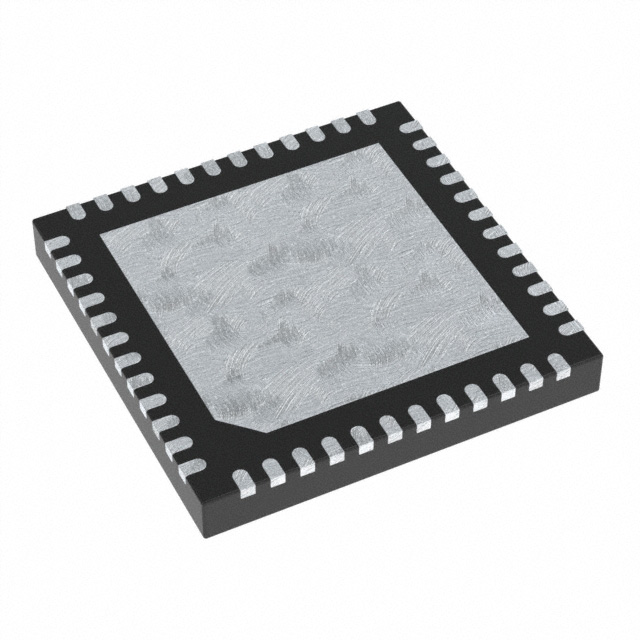
- Part No.:
- ATSAMR21G18A-MU
- Manufacturer:
- Microchip Technology
- Category:
- RF Transceiver ICs
- Package:
- 48-VFQFN Exposed Pad
- Datasheet:
-
 ATSAMR21G18A-MU.pdf
- Description:
- IC RF TXRX+MCU ISM>1GHZ 48QFN
- Quantity:
- Payment:

- Shipping:

Inventory:331
Please send an inquiry. Send us your inquiry, and we will respond immediately.
Product details
Overview
ATSAMR21G18A-MU from Microchip Technology (formerly Atmel) is a 32-bit ARM Cortex-M0+ wireless microcontroller integrating an ultra-low-power 2.4GHz ISM band transceiver, 256KB Flash, 32KB SRAM, and USB 2.0 interface. It operates at up to 48MHz, supports SleepWalking peripherals for autonomous operation in standby mode, and targets battery-powered IoT sensor nodes and mesh network endpoints.
For engineers reviewing the ATSAMR21G18A-MU datasheet, ATSAMR21G18A-MU pinout, ATSAMR21G18A-MU application, or ATSAMR21G18A-MU equivalent, key selection criteria include its QFN48 package with 28 GPIOs, integrated RF transceiver with -99dBm RX sensitivity and +4dBm TX output, hardware-assisted MAC, and support for capacitive touch and 12-bit ADC with oversampling up to 16-bit resolution.
Technical Context
The ATSAMR21G18A-MU implements a single-core ARM Cortex-M0+ processor with Thumb-2 ISA, 48MHz max clock, and Micro Trace Buffer (MTB) for non-intrusive debug. Its system architecture features three independent AHB-APB bridges, a 12-channel DMA controller, and a 12-channel Event System enabling inter-peripheral signaling without CPU intervention.
RF functionality is provided by an integrated 2.4GHz transceiver derived from the AT86RF233, supporting 250kb/s O-QPSK modulation, hardware CRC-16, auto-acknowledge, antenna diversity control, and dedicated SERCOM4 interface. Clocking includes DFLL48M and FDPLL96M PLLs, dual crystal oscillators (16MHz RF and 32.768kHz RTC), and multiple low-power internal sources.
Key Specifications
| Parameter | Value and Actual Design Meaning |
|---|---|
| CPU Core | ARM Cortex-M0+, 48MHz max - delivers 2.14 CoreMark/MHz efficiency for deterministic real-time control in power-constrained edge devices. |
| Memory | 256KB Flash / 32KB SRAM - sufficient for full Zigbee/Thread stack + application firmware with over-the-air update capability via SWD or USB bootloader. |
| RF Transceiver | 2.4GHz ISM band, -99dBm RX sensitivity, +4dBm TX output - enables reliable 100+ meter line-of-sight range in IEEE 802.15.4-compliant networks. |
| ADC | 12-bit, 350ksps, 8-channel, with 1x–16x programmable gain and hardware oversampling to 16-bit - supports high-accuracy analog sensing without external signal conditioning. |
| Low-Power Modes | Idle and standby modes with SleepWalking - allows peripherals (e.g., ADC, RTC, event system) to operate autonomously while CPU remains powered down, extending battery life to years. |
| USB Interface | Full-speed (12Mbps) USB 2.0 with embedded host/device capability and 8 endpoints - enables direct PC connectivity for configuration, firmware updates, or peripheral bridging without external PHY. |
| Operating Voltage | 1.8V–3.6V - compatible with single-cell Li-ion, LiPo, or two-cell alkaline batteries without external regulation. |
Pinout & Package
ATSAMR21G18A-MU is housed in a 48-pin QFN package (7mm × 7mm, 0.5mm pitch) with an exposed thermal pad internally connected to GND. The package complies with JEDEC MO-220, MSL3, and supports standard reflow per J-STD-20.
| Pin/Terminal | Circuit Role | Design Meaning |
|---|---|---|
| PA00 / PA01 | XIN32 / XOUT32 | 32.768kHz crystal oscillator inputs for RTC calendar accuracy and low-power wake-up timing. |
| XTAL1 / XTAL2 | 16MHz RF crystal interface | Dedicated pins for external crystal driving the integrated 2.4GHz transceiver's frequency synthesis. |
| RFP / RFN | Differential RF antenna interface | 50Ω matched differential outputs directly connect to balun or RF switch; require impedance-controlled PCB layout. |
| PA14 / PA15 | SERCOM4 MOSI / SCLK | Hardwired internal connection to AT86RF233 digital interface - no external routing needed for RF control. |
| PA30 / PA31 | SWCLK / SWDIO | Two-pin Serial Wire Debug interface - enables programming, non-intrusive trace, and real-time variable inspection using standard ARM debug tools. |
| GND (Pins 13,14,20,29,35) | Digital/analog ground planes | Multiple dedicated GND pins minimize noise coupling between RF, analog, and digital domains; center thermal pad must be soldered to PCB ground plane. |
Key Features
| Feature | Design Value |
|---|---|
| Integrated 2.4GHz Transceiver | Eliminates external RF IC and associated RF layout complexity; includes hardware MAC, CRC, auto-retry, and antenna diversity control for robust mesh networking. |
| Atmel Event System | Enables zero-latency, CPU-free peripheral chaining (e.g., timer triggers ADC, ADC result triggers DMA transfer), reducing active time and power consumption. |
| SleepWalking Peripherals | Allows RTC, ADC, or comparators to execute predefined sequences (e.g., periodic temperature sampling → threshold check → wake CPU only on alarm) while CPU remains in deep sleep. |
| Peripheral Touch Controller (PTC) | Supports up to 48 capacitive touch channels with proximity detection - enables intuitive HMI on battery-powered devices without dedicated touch IC. |
| Hardware AES & TRNG | On-chip cryptographic acceleration and true random number generation enable secure key derivation and encrypted OTA updates without software overhead or external security elements. |
Applications
| Smart Home Sensor Node | Industrial Wireless Monitor |
|---|---|
Use Scenario: Battery-powered temperature/humidity/motion sensor reporting to a Zigbee coordinator every 5 minutes. IC Role / Device Role / Timing Role: Primary SoC handling sensor acquisition, RF packet assembly, IEEE 802.15.4 MAC layer, and ultra-low-power scheduling via RTC and SleepWalking. Use Value: 256KB Flash stores full Zigbee PRO stack; -99dBm sensitivity ensures reliable reception in multi-wall environments; 1.8V operation extends CR2032 battery life beyond 2 years. | Use Scenario: DIN-rail mounted vibration/temperature monitor transmitting data via Thread to gateway in factory setting. IC Role / Device Role / Timing Role: Real-time data acquisition engine with hardware timestamping (RTC + TC), deterministic RF transmission, and fault-tolerant USB recovery interface. Use Value: USB device mode allows field technicians to reflash firmware or extract logs without opening enclosure; TCC modules generate precise PWM for LED status indicators synchronized to sensor events. |
| Wireless Lighting Control | Capacitive Touch Remote |
Use Scenario: BLE/Zigbee-enabled RGBW LED driver module controlling color, intensity, and scene transitions. IC Role / Device Role / Timing Role: Motor/lighting control MCU executing synchronized PWM across multiple channels using TCC modules with dead-time insertion and dithering. Use Value: Four TCC compare channels per instance drive high-efficiency MOSFET gates; hardware dithering increases effective PWM resolution to 16-bit, eliminating visible flicker at low brightness. | Use Scenario: Coin-cell powered remote with slider, wheel, and button controls for audio/video systems. IC Role / Device Role / Timing Role: Capacitive touch interface processor managing PTC scanning, proximity wake-up, and RF transmission of gesture data. Use Value: 48-channel PTC supports complex UIs; SleepWalking wakes PTC on proximity, scans only active zones, and transmits result - achieving sub-1µA average current in standby. |
Equivalent & Alternatives
The following parts are listed as comparable options for similar wireless microcontroller applications.
| Alternative Part | Technical Difference | Application Difference | Selection Advice |
|---|---|---|---|
| ATSAMR21E18A-MU | 32-pin QFN, 16 GPIOs, no XOSC32K, reduced SERCOM count (4 vs 5), same core/peripherals except PTC (6×2 vs 8×6) | Targeted at space-constrained designs where RF range and touch channel count are secondary to footprint and cost | Select when board area is critical and full 48-pin I/O or RTC crystal support is unnecessary. |
| nRF52840-QIAA | ARM Cortex-M4F, Bluetooth 5.0/802.15.4/Thread, 1MB Flash/256KB RAM, no integrated USB device stack, different pinout and power architecture | Better suited for Bluetooth-centric applications requiring higher compute throughput or larger code size; lacks native USB device interface | Choose when Bluetooth LE audio or concurrent multiprotocol operation is required, and USB device functionality is handled externally. |
Compared with ATSAMR21G18A-MU, ATSAMR21E18A-MU reduces I/O and RTC precision for smaller form factor, while nRF52840-QIAA trades integrated USB and SleepWalking autonomy for higher radio protocol flexibility and processing headroom - making each optimal for distinct system-level priorities.
Availability
ATSAMR21G18A-MU is available at Aetrix Electronics and suitable for smart home sensor nodes, industrial wireless monitors, wireless lighting controllers, and capacitive touch remotes requiring stable component supply and long-term production continuity.
Supply support for ATSAMR21G18A-MU includes scheduled delivery planning, volume procurement assistance, BOM continuity management, traceable sourcing, and lifecycle availability coordination for OEM customers, industrial embedded developers, connected-device designers, and electronics production programs.
Manufacturer
Microchip Technology acquired Atmel in 2016 and maintains full support for the SMART SAM portfolio, delivering high-reliability microcontrollers for industrial, automotive, and IoT applications.
The SAM R21 product line was designed specifically for ultra-low-power wireless embedded systems requiring integrated RF, deterministic real-time control, and seamless migration paths within the SAM family - emphasizing energy efficiency, hardware-accelerated peripherals, and simplified RF certification.
FAQ
What is the maximum operating frequency and process node of the ATSAMR21G18A-MU?
The ATSAMR21G18A-MU operates at a maximum frequency of 48MHz and is fabricated on a mature low-power CMOS process optimized for energy efficiency rather than nanometer scaling. Its ARM Cortex-M0+ core achieves 2.14 CoreMark/MHz, reflecting architectural efficiency over raw transistor density. This design prioritizes consistent low-voltage operation (1.8V–3.6V) and thermal stability in unregulated battery-powered environments - characteristics validated across its -40°C to +85°C industrial temperature range.
Does the ATSAMR21G18A-MU support USB device mode without external components?
Yes, the ATSAMR21G18A-MU integrates a full-speed USB 2.0 transceiver with embedded device stack support, requiring only a USB connector and appropriate ESD protection. It does not need an external PHY or level shifter. The internal USB module supports all standard descriptors and classes (CDC, HID, MSC), and firmware can implement custom class drivers. USB enumeration and data transfer occur directly through the on-chip DP/DM pins (PA24/PA25), with VBUS detection handled via software-configurable GPIO - enabling self-powered or bus-powered configurations without additional ICs.
How does the SleepWalking feature function in the ATSAMR21G18A-MU?
SleepWalking in the ATSAMR21G18A-MU allows selected peripherals - such as the RTC, ADC, or analog comparators - to operate autonomously in standby mode without waking the CPU. For example, the RTC can trigger the ADC to sample a thermistor every 30 seconds; the ADC result is compared against a threshold in hardware, and only if exceeded does the event system wake the CPU. This sequence executes entirely in hardware using preconfigured event paths, reducing average current to sub-1µA while maintaining responsiveness - a capability confirmed in the preliminary datasheet summary and verified in Atmel application note AVR1312.
What RF certifications apply to the ATSAMR21G18A-MU's integrated transceiver?
The integrated 2.4GHz transceiver in the ATSAMR21G18A-MU is based on the AT86RF233 silicon and supports FCC Part 15.247, IC RSS-247, CE RED, and ETSI EN 300 328 compliance when used with approved reference antennas and layout guidelines. Certification is system-level and requires validation of the final PCB antenna design, matching network, and enclosure. Microchip provides pre-certified reference designs (e.g., ATSAMR21-XPRO) and test reports to accelerate regulatory approval - but standalone ATSAMR21G18A-MU modules do not carry individual modular certification.
Can the ATSAMR21G18A-MU's ADC achieve true 16-bit resolution, and how is it implemented?
Yes, the ATSAMR21G18A-MU's 12-bit ADC achieves effective 16-bit resolution through hardware oversampling and decimation - specifically 256× oversampling yielding 16-bit output at 1.37ksps. This is not interpolation; it is statistically valid noise-shaping where quantization noise is pushed out of band and filtered digitally. The process is fully autonomous: oversampling ratio, decimation filter type (SINC2/SINC3), and gain stage (1x–16x) are configured in registers, and results appear directly in memory via DMA - enabling high-precision sensor measurements without CPU involvement or external delta-sigma converters.
ATSAMR21G18A-MU Specifications
- Product attributes
- Attribute value
- Manufacturer:
- Microchip Technology
- Series:
- SMART™ SAM R21
- Package/Case:
- 48-VFQFN Exposed Pad
- Packaging:
- Tray
- Product Status:
- Active
- Programmable:
- Not Verified
- Type:
- TxRx + MCU
- RF Family/Standard:
- General ISM > 1GHz
- Protocol:
- -
- Modulation:
- O-QPSK
- Frequency:
- 2.4GHz
- Data Rate (Max):
- 250kbps
- Power - Output:
- 4dBm
- Sensitivity:
- -99dBm
- Memory Size:
- 256kB Flash, 32kB SRAM
- Serial Interfaces:
- I2C, SPI, UART, USART, USB
- GPIO:
- 28
- Voltage - Supply:
- 1.8V ~ 3.6V
- Current - Receiving:
- 11.3mA ~ 11.8mA
- Current - Transmitting:
- 7.2mA ~ 13.8mA
- Operating Temperature:
- -40°C ~ 85°C
- Grade:
- -
- Qualification:
- -
- Supplier Device Package:
- 48-QFN (7x7)
ATSAMR21G18A-MU FAQ
1.How can I place an order for ATSAMR21G18A-MU through Aetrix?
Please submit a Request for Quotation (RFQ) for ATSAMR21G18A-MU on Aetrix. Our sales agent will provide a competitive quotation and guide you through the order confirmation once you accept the terms.
2.Are the price and stock information for ATSAMR21G18A-MU reliable?
The price and inventory of ATSAMR21G18A-MU are updated periodically and may fluctuate due to market conditions. Stock and pricing data are typically refreshed every 24 hours. Quotation validity for ATSAMR21G18A-MU is usually 5 days.
3.What payment methods are accepted for ATSAMR21G18A-MU?
We accept Wire Transfer, PayPal, Credit Card, Western Union, MoneyGram, and Escrow for ATSAMR21G18A-MU transactions.
Note: Certain payment methods may incur a processing fee.
4.How is shipping managed for ATSAMR21G18A-MU?
ATSAMR21G18A-MU orders can be shipped via leading logistics carriers, including DHL, UPS, FedEx, TNT, or Registered Mail.
Once your ATSAMR21G18A-MU order is processed, you will receive an email with the shipment details and tracking number.
Note: Tracking information may take up to 24 hours to appear. Express delivery typically takes 3–5 business days.
5.How can I obtain technical support or documentation for ATSAMR21G18A-MU?
For technical support, including ATSAMR21G18A-MU datasheets, pinout diagrams, or application guidance, please contact our engineering support team. They can provide detailed documentation and assistance for your ATSAMR21G18A-MU requirements.
6.How does Aetrix verify that ATSAMR21G18A-MU is sourced from the original manufacturer or authorized distributors?
All ATSAMR21G18A-MU products on Aetrix are procured from qualified distributors and authorized channels. Our dedicated quality assurance team conducts strict verification, including traceability checks and, if necessary, third-party testing. This ensures that ATSAMR21G18A-MU meets industry standards.
7.What is the process for return or replacement of ATSAMR21G18A-MU?
All ATSAMR21G18A-MU units undergo pre-shipment inspection (PSI). If there is an issue with ATSAMR21G18A-MU, returns or replacements are accepted under the following conditions:
1.Quantity discrepancies, incorrect items, or visible external defects (such as breakage or corrosion), acknowledged by Aetrix.
2.The issue is reported within 90 days of delivery.
3.The ATSAMR21G18A-MU part is unused and in its original packaging.
Return procedure for ATSAMR21G18A-MU:
1.Submit a request within 90 days.
2.Obtain a Return Material Authorization (RMA) from Aetrix.
ATSAMR21G18A-MU Tags

-
ESP32-D0WD-V3
Espressif Systems

-
ESP8266EX
Espressif Systems

-
ESP32-S3
Espressif Systems

-
NRF24L01P-R7
Nordic Semiconductor ASA
-
NRF24L01P-R
Nordic Semiconductor ASA

-
ESP32-U4WDH
Espressif Systems

-
DA14531-00000OG2
Renesas
-
ESP32-C6FH4
Espressif Systems

-
DA14531-00000FX2
Renesas
-
NRF24L01P-T
Nordic Semiconductor ASA

-
NRF52810-QCAA-R
Nordic Semiconductor ASA
-
ESP32-S3FN8
Espressif Systems
Tech Hub

TTL and CMOS logic families differ in thresholds, loading, output drive, power and timing. This engineering guide compares 74HC and 74HCT, calculates noise margins and checks 3.3 V/5 V compatibility.

A practical engineering guide to 3.3V and 5V logic compatibility, input thresholds, resistor dividers, translator ICs, MOSFET level shifting, I2C pull-ups, timing limits and power-sequencing risks.

The 74HC595 uses push-pull logic outputs, while the TPIC6B595 uses 50 V open-drain DMOS sinks for higher-power loads. This guide compares timing, current limits, 3.3 V interfacing, load wiring, thermal…

The 74HC595 converts serial data into eight stable parallel outputs. This guide covers pin functions, shift and storage timing, OE and MR behavior, drive-current limits, cascading, voltage compatibilit…

A technical comparison of level-sensitive latches and edge-triggered flip-flops, covering timing windows, setup and hold limits, master–slave operation, time borrowing, race-through, HDL inference and…

A D latch stores one bit while Enable controls when data can pass. This reference covers gate-level operation, truth tables, transparency, setup and hold timing, LE versus OE, common ICs and practical …

An SR latch stores one bit through cross-coupled feedback. This engineering reference covers NOR and NAND implementations, truth tables, forbidden-state recovery, gated operation, switch debouncing, fa…

Latch circuits retain one bit through feedback. This technical reference covers SR and D latches, truth tables, transparency, timing limits, latch-versus-flip-flop behavior, applications and common log…

An engineering guide to LED driver operation, constant-current and constant-voltage outputs, linear and switching topologies, dimming, IC selection, calculations, replacement compatibility, and fault c…

Operational amplifier guide covering op amp basics, feedback, ideal vs real op amps, common configurations, buffer circuits, offset, bias current, gain-bandwidth, slew rate, rail-to-rail limits and sel…


